AMD Radeon R9 390X vs NVIDIA GeForce GTX 1070
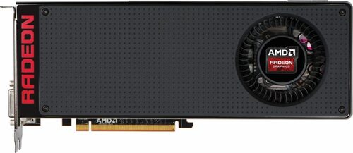
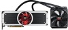
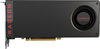
AMD Radeon R9 390X
$429
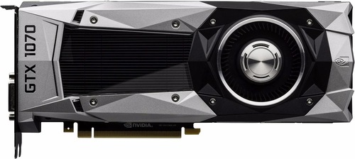
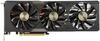
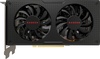
NVIDIA GeForce GTX 1070
$449
|
2816 Shaders
8GB GDDR5
1050MHz
|
1920 Shaders
8GB GDDR5
1683MHz
|
|
Peak AI Performance
5.91 TFLOPS
FP32
|
Peak AI Performance
25.85 TOPS
INT8
|
|
FP32
5.91 TFLOPS
|
FP32
6.46 TFLOPS
|
|
-
-
|
FP16
100 GFLOPS
|
|
Form Factor
PCIe Card
2.0-Slots
|
Form Factor
PCIe Card
2.0-Slots
|
|
TDP
275W
|
TDP
150W
|
|
Power Connectors
1x 6-Pin
1x 8-Pin
-
-
|
Power Connectors
-
1x 8-Pin
-
-
|
|
GB6 Metal N/A
0%
|
GB6 Metal N/A
0%
|
|
GB6 Vulkan N/A
0%
|
|
GB5 OpenCL N/A
0%
|
GB5 OpenCL N/A
0%
|
|
GB5 CUDA N/A
0%
|
GB5 CUDA N/A
0%
|
|
GB5 Metal N/A
0%
|
GB5 Metal N/A
0%
|
|
GB5 Vulkan N/A
0%
|
GB5 Vulkan N/A
0%
|
|
OCT 2020.1 N/A
0%
|
OCT 2020.1 N/A
0%
|
|
OCT Metal N/A
0%
|
OCT Metal N/A
0%
|
|
Peak AI
Performance
5.91 TFLOPS
FP32
|
Peak AI
Performance
25.85 TOPS
INT8
|
|
-
-
-
|
-
-
-
|
|
-
-
-
-
-
-
|
-
-
-
-
-
-
|
|
-
-
-
-
-
-
|
FP16
100 GFLOPS
-
-
-
-
|
|
FP32
5.91 TFLOPS
-
-
|
FP32
6.46 TFLOPS
-
-
|
|
FP64
740 GFLOPS
-
|
FP64
200 GFLOPS
-
|
|
-
-
-
-
|
-
-
-
-
|
|
-
-
-
|
-
-
-
|
|
-
-
-
|
-
-
-
|
|
-
-
-
-
|
INT8
25.85 TOPS
-
-
|
|
-
-
|
-
-
|
|
-
-
|
-
-
|
|
Pixel
Fillrate
67.2 GPixel/s
|
Pixel
Fillrate
107.712 GPixel/s
|
|
-
-
|
-
-
|
|
Texture
Fillrate
184.8 GTexel/s
|
Texture
Fillrate
201.96 GTexel/s
|
|
Manufacturer
AMD
|
Manufacturer
NVIDIA
|
|
Chip Designer
AMD
|
Chip Designer
NVIDIA
|
|
Architecture
GCN 2
|
Architecture
Pascal
|
|
Family
Radeon R 300
|
Family
GeForce 10
|
|
Codename
Hawaii
-
Variant
Grenada XT
|
Codename
NV134
GP104
Variant
GP104-200-A1
|
|
Market Segment
Desktop
|
Market Segment
Desktop
|
|
Release Date
6/18/2015
|
Release Date
6/10/2016
|
|
Foundry
TSMC
-
|
Foundry
TSMC
-
|
|
Fabrication Node
28nm
-
|
Fabrication Node
16FF
-
|
|
Die Size
438 mm²
-
|
Die Size
314 mm²
-
|
|
Transistor Count
6.2 Billion
-
|
Transistor Count
7.2 Billion
-
|
|
Transistor Density
14.16M/mm²
-
|
Transistor Density
22.93M/mm²
-
|
|
Form
PCIe Card
|
Form
PCIe Card
|
|
Shading Units
2816 Shaders
-
|
Shading Units
1920 Shaders
-
|
|
Texture Mapping Units
176 TMUs
|
Texture Mapping Units
120 TMUs
|
|
Render Output Units
64 ROPs
|
Render Output Units
64 ROPs
|
|
-
-
|
-
-
|
|
-
-
|
-
-
|
|
-
-
|
Streaming Multiprocessors
15 SMs
|
|
Compute Units
44 CUs
|
-
-
|
|
-
-
|
-
-
|
|
-
-
|
Graphics Processing Clusters
3 GPCs
|
|
-
-
-
1050MHz
|
-
-
1506MHz Base
1683MHz
|
|
-
-
|
-
-
|
|
L1
-
-
16KB/CU
-
|
L1
-
48KB/SM
-
-
|
|
L2
1MB Shared
|
L2
2MB Shared
|
|
-
-
-
|
-
-
-
|
|
8GB
GDDR5
-
|
8GB
GDDR5
-
|
|
Bus Width
512Bit
|
Bus Width
256Bit
|
|
Clock
1500MHz
Transfer Rate
6GT/s
Bandwidth
384GB/s
|
Clock
2000MHz
Transfer Rate
8GT/s
Bandwidth
256GB/s
|
|
-
-
-
-
-
-
-
-
-
|
-
-
-
-
-
-
-
-
-
|
|
TDP
275W
|
TDP
150W
|
|
-
-
|
-
-
|
|
-
-
-
-
-
-
-
-
-
-
2x DVI-D Dual-Link
-
-
-
-
-
-
-
-
-
-
-
1x DisplayPort 1.2
-
-
-
-
-
-
-
-
-
-
-
1x HDMI 1.4
-
-
-
-
|
-
-
-
-
-
-
-
-
-
-
1x DVI-D Dual-Link
-
-
-
-
-
-
-
-
-
-
-
-
-
3x DisplayPort 1.4
-
-
-
-
-
-
-
-
-
-
1x HDMI 2.0
-
-
-
|
|
Max Resolution
4096x2160
|
Max Resolution
7680x4320
|
|
Max Resolution Refresh Rate
60Hz
|
Max Resolution Refresh Rate
30Hz
|
|
Variable Refresh Rate
-
FreeSync
-
|
Variable Refresh Rate
G-Sync
FreeSync
-
|
|
Display Stream Compression (DSC)
Not Supported
|
Display Stream Compression (DSC)
Not Supported
|
|
Multi Monitor Support
3
|
Multi Monitor Support
3
|
|
Content Protection
HDCP 1.4
|
-
-
|
|
Model
VCE 2.0
|
Model
2x NVENC 4
|
|
Codec
-
-
-
-
-
-
-
-
AVC (H.264)
-
-
-
-
-
|
Codec
-
-
-
-
-
-
-
-
AVC (H.264)
HEVC (H.265)
-
-
-
-
|
|
Model
UVD 4.2
|
Model
NVDEC 3
|
|
Codec
MPEG-1
MPEG-2
MPEG-4
-
VC-1
-
-
-
AVC (H.264)
-
-
-
-
-
|
Codec
MPEG-1
MPEG-2
MPEG-4
-
VC-1
-
VP9
-
AVC (H.264)
HEVC (H.265)
-
-
-
-
|
|
Direct X
12
Direct 3D
12_0
|
Direct X
12
Direct 3D
12_1
|
|
OpenGL
4.6
OpenCL
2.1
Vulkan
1.2
|
OpenGL
4.6
OpenCL
3.0
Vulkan
1.3
|
|
Shader Model
6.5
-
-
GFX
7
-
-
-
-
|
Shader Model
6.7
CUDA
6.1
-
-
PureVideo HD
VP8
VDPAU
Feature Set H
|
|
-
-
-
1x Fan
|
-
-
-
1x Fan
|
|
Power Connectors
-
-
1x 6-Pin
1x 8-Pin
-
-
-
|
Power Connectors
-
-
-
1x 8-Pin
-
-
-
|
|
Slots Required
2.0
PCIe Version
3.0
PCIe Lanes
16
|
Slots Required
2.0
PCIe Version
3.0
PCIe Lanes
16
|
|
Multi GPU Support
Supported
Type
CrossFire XDMA
|
Multi GPU Support
Supported
Type
4-way SLI - 2-way SLI HB
|
|
Height
110 mm (4.33 in)
Width
275 mm (10.83 in)
Depth
36 mm (1.42 in)
|
Height
112 mm (4.41 in)
Width
267 mm (10.51 in)
Depth
40 mm (1.57 in)
|


Copy Link