ATI Radeon HD 4700 vs NVIDIA GeForce GT 430 2GB
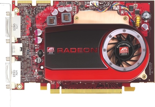
ATI Radeon HD 4700

NVIDIA GeForce GT 430 2GB
$79
|
320 Shaders
512MB DDR2
600MHz
|
96 Shaders
2GB GDDR3
700MHz
|
|
Peak AI Performance
380 GFLOPS
FP32
|
Peak AI Performance
0.27 TOPS
INT32
|
|
FP32
380 GFLOPS
|
FP32
270 GFLOPS
|
|
-
-
|
-
-
|
|
Form Factor
PCIe Card
1.0-Slots
|
Form Factor
PCIe Card
1.0-Slots
|
|
TDP
59W
|
TDP
49W
|
|
Power Connectors
1x 6-Pin
-
-
-
|
-
-
-
-
-
|
|
GB6 OpenCL N/A
0%
|
GB6 OpenCL N/A
0%
|
|
GB6 Metal N/A
0%
|
GB6 Metal N/A
0%
|
|
GB6 Vulkan N/A
0%
|
GB6 Vulkan N/A
0%
|
|
GB5 OpenCL N/A
0%
|
GB5 OpenCL N/A
0%
|
|
GB5 CUDA N/A
0%
|
GB5 CUDA N/A
0%
|
|
GB5 Metal N/A
0%
|
GB5 Metal N/A
0%
|
|
GB5 Vulkan N/A
0%
|
GB5 Vulkan N/A
0%
|
|
OCT 2020.1 N/A
0%
|
OCT 2020.1 N/A
0%
|
|
OCT Metal N/A
0%
|
OCT Metal N/A
0%
|
|
Peak AI
Performance
380 GFLOPS
FP32
|
Peak AI
Performance
0.27 TOPS
INT32
|
|
-
-
-
|
-
-
-
|
|
-
-
-
-
-
-
|
-
-
-
-
-
-
|
|
-
-
-
-
-
-
|
-
-
-
-
-
-
|
|
FP32
380 GFLOPS
-
-
|
FP32
270 GFLOPS
-
-
|
|
FP64
80 GFLOPS
-
|
FP64
20 GFLOPS
-
|
|
-
-
-
-
|
-
-
-
-
|
|
-
-
-
|
-
-
-
|
|
-
-
-
|
-
-
-
|
|
-
-
-
-
|
-
-
-
-
|
|
-
-
|
INT32
0.27 TOPS
|
|
-
-
|
-
-
|
|
Pixel
Fillrate
4.8 GPixel/s
|
Pixel
Fillrate
2.8 GPixel/s
|
|
-
-
|
-
-
|
|
Texture
Fillrate
19.2 GTexel/s
|
Texture
Fillrate
11.2 GTexel/s
|
|
Manufacturer
ATI
|
Manufacturer
NVIDIA
|
|
Chip Designer
ATI
|
Chip Designer
NVIDIA
|
|
Architecture
TeraScale 1
|
Architecture
Fermi
|
|
Family
Radeon HD 4000
|
Family
GeForce 400
|
|
Codename
Wekiva
RV770
Variant
RV770 CE
|
Codename
NVC1
GF108
Variant
GF108-300-A1
|
|
Market Segment
Desktop
|
Market Segment
Desktop
|
|
Release Date
2/11/2009
|
Release Date
10/11/2010
|
|
Foundry
TSMC
-
|
Foundry
TSMC
-
|
|
Fabrication Node
55nm
-
|
Fabrication Node
40nm
-
|
|
Die Size
256 mm²
-
|
Die Size
116 mm²
-
|
|
Transistor Count
956 Million
-
|
Transistor Count
585 Million
-
|
|
Transistor Density
3.73M/mm²
-
|
Transistor Density
5.04M/mm²
-
|
|
Form
PCIe Card
|
Form
PCIe Card
|
|
Shading Units
320 Shaders
-
|
Shading Units
96 Shaders
-
|
|
Texture Mapping Units
32 TMUs
|
Texture Mapping Units
16 TMUs
|
|
Render Output Units
8 ROPs
|
Render Output Units
4 ROPs
|
|
-
-
|
-
-
|
|
-
-
|
-
-
|
|
-
-
|
Streaming Multiprocessors
2 SMs
|
|
Compute Units
8 CUs
|
-
-
|
|
-
-
|
-
-
|
|
-
-
|
-
-
|
|
-
-
-
600MHz
|
-
1400MHz Shader
-
700MHz
|
|
-
-
|
-
-
|
|
L1
-
-
16KB/CU
-
|
L1
-
64KB/SM
-
-
|
|
L2
256KB Shared
|
L2
256KB Shared
|
|
-
-
-
|
-
-
-
|
|
512MB
DDR2
-
|
2GB
GDDR3
-
|
|
Bus Width
128Bit
|
Bus Width
128Bit
|
|
Clock
400MHz
Transfer Rate
800MT/s
Bandwidth
12.8GB/s
|
Clock
900MHz
Transfer Rate
1.8GT/s
Bandwidth
28.8GB/s
|
|
-
-
-
-
-
-
-
-
-
|
-
-
-
-
-
-
-
-
-
|
|
TDP
59W
|
TDP
49W
|
|
-
-
|
-
-
|
|
-
1x S-Video
-
-
-
-
-
-
2x DVI-I Dual-Link
-
-
-
-
-
-
-
-
-
-
-
-
-
-
-
-
-
-
-
-
-
-
-
-
-
-
-
-
-
-
|
1x VGA
-
-
-
-
-
-
-
1x DVI-I Dual-Link
-
-
-
-
-
-
-
-
-
-
-
-
-
-
-
-
-
-
-
-
-
-
-
-
1x HDMI 1.3
-
-
-
-
-
|
|
Max Resolution
2560x1600
|
Max Resolution
2560x1600
|
|
Max Resolution Refresh Rate
60Hz
|
Max Resolution Refresh Rate
60Hz
|
|
Variable Refresh Rate
-
-
-
|
Variable Refresh Rate
-
-
-
|
|
Display Stream Compression (DSC)
Not Supported
|
Display Stream Compression (DSC)
Not Supported
|
|
Multi Monitor Support
2
|
Multi Monitor Support
2
|
|
-
-
|
-
-
|
|
No Encoders
-
|
No Encoders
-
|
|
-
-
-
-
-
-
-
-
-
-
-
-
-
-
-
|
-
-
-
-
-
-
-
-
-
-
-
-
-
-
-
|
|
Model
UVD 2.0
|
No Decoders
|
|
Codec
-
-
-
-
VC-1
-
-
-
AVC (H.264)
-
-
-
-
-
|
-
-
-
-
-
-
-
-
-
-
-
-
-
-
|
|
Direct X
10
Direct 3D
10_1
|
Direct X
12
Direct 3D
11_0
|
|
OpenGL
3.3
OpenCL
1.1
-
-
|
OpenGL
4.6
OpenCL
1.1
-
-
|
|
Shader Model
4.1
-
-
GFX
3
-
-
-
-
|
Shader Model
5.1
CUDA
2.1
-
-
PureVideo HD
VP4
VDPAU
Feature Set C
|
|
-
-
-
1x Fan
|
-
-
-
1x Fan
|
|
Power Connectors
-
-
1x 6-Pin
-
-
-
-
|
-
-
-
-
-
-
-
-
|
|
Slots Required
1.0
PCIe Version
2.0
PCIe Lanes
16
|
Slots Required
1.0
PCIe Version
2.0
PCIe Lanes
16
|
|
Multi GPU Support
Supported
Type
2-way CrossFireX
|
-
-
-
-
|
|
-
-
-
-
-
-
|
Height
69 mm (2.72 in)
Width
145 mm (5.71 in)
Depth
20 mm (0.79 in)
|


Copy Link