ATI Radeon HD 4750 vs ATI Radeon HD 4870 X2
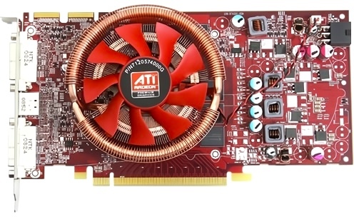
ATI Radeon HD 4750
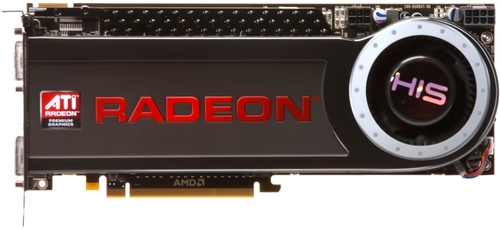
ATI Radeon HD 4870 X2
$449
|
640 Shaders
512MB GDDR5
730MHz
|
2x 800 Shaders
2GB (2x 1GB) GDDR5
750MHz
|
|
Peak AI Performance
930 GFLOPS
FP32
|
Peak AI Performance
2.4 TFLOPS
FP32
|
|
FP32
930 GFLOPS
|
FP32
2.4 TFLOPS
|
|
-
-
|
-
-
|
|
Form Factor
PCIe Card
1.0-Slots
|
Form Factor
PCIe Card
2.0-Slots
|
|
TDP
80W
|
TDP
286W
|
|
Power Connectors
1x 6-Pin
-
-
-
|
Power Connectors
1x 6-Pin
1x 8-Pin
-
-
|
|
GB6 OpenCL N/A
0%
|
GB6 OpenCL N/A
0%
|
|
GB6 Metal N/A
0%
|
GB6 Metal N/A
0%
|
|
GB6 Vulkan N/A
0%
|
GB6 Vulkan N/A
0%
|
|
GB5 OpenCL N/A
0%
|
GB5 OpenCL N/A
0%
|
|
GB5 CUDA N/A
0%
|
GB5 CUDA N/A
0%
|
|
GB5 Metal N/A
0%
|
GB5 Metal N/A
0%
|
|
GB5 Vulkan N/A
0%
|
GB5 Vulkan N/A
0%
|
|
OCT 2020.1 N/A
0%
|
OCT 2020.1 N/A
0%
|
|
OCT Metal N/A
0%
|
OCT Metal N/A
0%
|
|
Peak AI
Performance
930 GFLOPS
FP32
|
Peak AI
Performance
2.4 TFLOPS
FP32
|
|
-
-
-
|
-
-
-
|
|
-
-
-
-
-
-
|
-
-
-
-
-
-
|
|
-
-
-
-
-
-
|
-
-
-
-
-
-
|
|
FP32
930 GFLOPS
-
-
|
FP32
2.4 TFLOPS
-
-
|
|
FP64
190 GFLOPS
-
|
FP64
480 GFLOPS
-
|
|
-
-
-
-
|
-
-
-
-
|
|
-
-
-
|
-
-
-
|
|
-
-
-
|
-
-
-
|
|
-
-
-
-
|
-
-
-
-
|
|
-
-
|
-
-
|
|
-
-
|
-
-
|
|
Pixel
Fillrate
11.68 GPixel/s
|
Pixel
Fillrate
12 GPixel/s
|
|
-
-
|
-
-
|
|
Texture
Fillrate
23.36 GTexel/s
|
Texture
Fillrate
30 GTexel/s
|
|
Manufacturer
ATI
|
Manufacturer
ATI
|
|
Chip Designer
ATI
|
Chip Designer
ATI
|
|
Architecture
TeraScale 1
|
Architecture
TeraScale 1
|
|
Family
Radeon HD 4000
|
Family
Radeon HD 4000
|
|
Codename
Walden
RV740
Variant
RV740
|
Codename
Wekiva
RV770
Variant
RV770 XT
|
|
Market Segment
Desktop
|
Market Segment
Desktop
|
|
Release Date
9/9/2009
|
Release Date
8/12/2008
|
|
Foundry
TSMC
-
|
Foundry
TSMC
-
|
|
Fabrication Node
40nm
-
|
Fabrication Node
55nm
-
|
|
Die Size
137 mm²
-
|
Die Size
2x 256 mm²
-
|
|
Transistor Count
826 Million
-
|
Transistor Count
2x 956 Million
-
|
|
Transistor Density
6.03M/mm²
-
|
Transistor Density
3.73M/mm²
-
|
|
Form
PCIe Card
|
Form
PCIe Card
|
|
Shading Units
640 Shaders
-
|
Shading Units
2x 800 Shaders
-
|
|
Texture Mapping Units
32 TMUs
|
Texture Mapping Units
2x 40 TMUs
|
|
Render Output Units
16 ROPs
|
Render Output Units
2x 16 ROPs
|
|
-
-
|
-
-
|
|
-
-
|
-
-
|
|
-
-
|
-
-
|
|
Compute Units
8 CUs
|
Compute Units
2x 10 CUs
|
|
-
-
|
-
-
|
|
-
-
|
-
-
|
|
-
-
-
730MHz
|
-
-
-
750MHz
|
|
-
-
|
-
-
|
|
L1
-
-
16KB/CU
-
|
L1
-
-
16KB/CU
-
|
|
L2
128KB Shared
|
L2
256KB Shared
|
|
-
-
-
|
-
-
-
|
|
512MB
GDDR5
-
|
2GB (2x 1GB)
GDDR5
-
|
|
Bus Width
128Bit
|
Bus Width
256Bit
|
|
Clock
800MHz
Transfer Rate
3.2GT/s
Bandwidth
51.2GB/s
|
Clock
900MHz
Transfer Rate
3.6GT/s
Bandwidth
115.2GB/s
|
|
-
-
-
-
-
-
-
-
-
|
-
-
-
-
-
-
-
-
-
|
|
TDP
80W
|
TDP
286W
|
|
-
-
|
-
-
|
|
-
1x S-Video
-
-
-
-
-
-
2x DVI-I Dual-Link
-
-
-
-
-
-
-
-
-
-
-
-
-
-
-
-
-
-
-
-
-
-
-
-
-
-
-
-
-
-
|
-
1x S-Video
-
-
-
-
-
-
2x DVI-I Dual-Link
-
-
-
-
-
-
-
-
-
-
-
-
-
-
-
-
-
-
-
-
-
-
-
-
-
-
-
-
-
-
|
|
Max Resolution
2560x1600
|
Max Resolution
2560x1600
|
|
Max Resolution Refresh Rate
60Hz
|
Max Resolution Refresh Rate
60Hz
|
|
Variable Refresh Rate
-
-
-
|
Variable Refresh Rate
-
-
-
|
|
Display Stream Compression (DSC)
Not Supported
|
Display Stream Compression (DSC)
Not Supported
|
|
Multi Monitor Support
2
|
Multi Monitor Support
2
|
|
-
-
|
-
-
|
|
No Encoders
-
|
No Encoders
-
|
|
-
-
-
-
-
-
-
-
-
-
-
-
-
-
-
|
-
-
-
-
-
-
-
-
-
-
-
-
-
-
-
|
|
Model
UVD 2.2
|
Model
UVD 2.0
|
|
Codec
-
-
-
-
VC-1
-
-
-
AVC (H.264)
-
-
-
-
-
|
Codec
-
-
-
-
VC-1
-
-
-
AVC (H.264)
-
-
-
-
-
|
|
Direct X
10
Direct 3D
10_1
|
Direct X
10
Direct 3D
10_1
|
|
OpenGL
3.3
OpenCL
1.1
-
-
|
OpenGL
3.3
OpenCL
1.1
-
-
|
|
Shader Model
4.1
-
-
GFX
3
-
-
-
-
|
Shader Model
4.1
-
-
GFX
3
-
-
-
-
|
|
-
-
-
1x Fan
|
-
-
-
1x Fan
|
|
Power Connectors
-
-
1x 6-Pin
-
-
-
-
|
Power Connectors
-
-
1x 6-Pin
1x 8-Pin
-
-
-
|
|
Slots Required
1.0
PCIe Version
2.0
PCIe Lanes
16
|
Slots Required
2.0
PCIe Version
2.0
PCIe Lanes
16
|
|
Multi GPU Support
Supported
Type
2-way CrossFireX
|
Multi GPU Support
Supported
Type
2-way CrossFireX
|
|
-
-
-
-
-
-
|
-
-
-
-
-
-
|


Copy Link