MSI GeForce RTX 3070 Gaming X Trio vs EVGA GeForce RTX 3070 XC3 Ultra
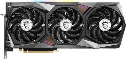
MSI GeForce RTX 3070 Gaming X Trio
$640
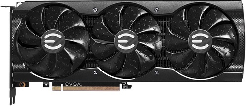
EVGA GeForce RTX 3070 XC3 Ultra
$560
|
5888 Shaders
8GB GDDR6
1830MHz
|
5888 Shaders
8GB GDDR6
1770MHz
|
|
Peak AI Performance
689.6 TOPS
INT4 Tensor Sparse
|
Peak AI Performance
666.99 TOPS
INT4 Tensor Sparse
|
|
FP32
21.55 TFLOPS
|
FP32
20.84 TFLOPS
|
|
FP16
21.55 TFLOPS
|
FP16
20.84 TFLOPS
|
|
Form Factor
PCIe Card
2.8-Slots
|
Form Factor
PCIe Card
2.1-Slots
|
|
TDP
220W
|
TDP
220W
|
|
Power Connectors
-
2x 8-Pin
-
-
|
-
-
-
-
-
|
|
GB6 OpenCL N/A
0%
|
GB6 OpenCL N/A
0%
|
|
GB6 Metal N/A
0%
|
GB6 Metal N/A
0%
|
|
GB6 Vulkan N/A
0%
|
GB6 Vulkan N/A
0%
|
|
GB5 OpenCL 143,235
47%
|
GB5 OpenCL 135,020
44%
|
|
GB5 CUDA 158,955
45%
|
GB5 CUDA 149,835
42%
|
|
GB5 Metal N/A
0%
|
GB5 Metal N/A
0%
|
|
GB5 Vulkan 106,320
52%
|
GB5 Vulkan 100,220
49%
|
|
OCT 2020.1 430
57%
|
OCT 2020.1 405
53%
|
|
OCT Metal N/A
0%
|
OCT Metal N/A
0%
|
|
Peak AI
Performance
689.6 TOPS
INT4 Tensor Sparse
|
Peak AI
Performance
666.99 TOPS
INT4 Tensor Sparse
|
|
-
-
-
|
-
-
-
|
|
-
-
-
-
-
-
|
-
-
-
-
-
-
|
|
FP16
21.55 TFLOPS
86.2 TFLOPS
Tensor (FP16 Accumulate)
172.4 TFLOPS
Tensor (FP16 Accumulate) Sparse
43.1 TFLOPS
Tensor (FP32 Accumulate)
86.2 TFLOPS
Tensor (FP32 Accumulate) Sparse
|
FP16
20.84 TFLOPS
83.37 TFLOPS
Tensor (FP16 Accumulate)
166.75 TFLOPS
Tensor (FP16 Accumulate) Sparse
41.69 TFLOPS
Tensor (FP32 Accumulate)
83.37 TFLOPS
Tensor (FP32 Accumulate) Sparse
|
|
FP32
21.55 TFLOPS
-
-
|
FP32
20.84 TFLOPS
-
-
|
|
FP64
340 GFLOPS
-
|
FP64
330 GFLOPS
-
|
|
BF16
21.55 TFLOPS
43.1 TFLOPS
Tensor
86.2 TFLOPS
Tensor Sparse
|
BF16
20.84 TFLOPS
41.69 TFLOPS
Tensor
83.37 TFLOPS
Tensor Sparse
|
|
TF32
21.55 TFLOPS
Tensor
43.1 TFLOPS
Tensor Sparse
|
TF32
20.84 TFLOPS
Tensor
41.69 TFLOPS
Tensor Sparse
|
|
INT4
344.8 TOPS
Tensor
689.6 TOPS
Tensor Sparse
|
INT4
333.5 TOPS
Tensor
666.99 TOPS
Tensor Sparse
|
|
INT8
-
172.4 TOPS
Tensor
344.8 TOPS
Tensor Sparse
|
INT8
-
166.75 TOPS
Tensor
333.5 TOPS
Tensor Sparse
|
|
INT32
10.78 TOPS
|
INT32
10.42 TOPS
|
|
Ray Tracing
32.5 TOPS
|
Ray Tracing
31.4 TOPS
|
|
Pixel
Fillrate
175.68 GPixel/s
|
Pixel
Fillrate
169.92 GPixel/s
|
|
-
-
|
-
-
|
|
Texture
Fillrate
336.72 GTexel/s
|
Texture
Fillrate
325.68 GTexel/s
|
|
Manufacturer
MSI
|
Manufacturer
EVGA
|
|
Chip Designer
NVIDIA
|
Chip Designer
NVIDIA
|
|
Architecture
Ampere
|
Architecture
Ampere
|
|
Family
GeForce 30
|
Family
GeForce 30
|
|
Codename
NV174
GA104
Variant
GA104-300-A1
|
Codename
NV174
GA104
Variant
GA104-300-A1
|
|
Market Segment
Desktop
|
Market Segment
Desktop
|
|
Release Date
10/29/2020
|
Release Date
10/29/2020
|
|
Foundry
Samsung
-
|
Foundry
Samsung
-
|
|
Fabrication Node
8N
-
|
Fabrication Node
8N
-
|
|
Die Size
393 mm²
-
|
Die Size
393 mm²
-
|
|
Transistor Count
17.4 Billion
-
|
Transistor Count
17.4 Billion
-
|
|
Transistor Density
44.33M/mm²
-
|
Transistor Density
44.33M/mm²
-
|
|
Form
PCIe Card
|
Form
PCIe Card
|
|
Shading Units
5888 Shaders
-
|
Shading Units
5888 Shaders
-
|
|
Texture Mapping Units
184 TMUs
|
Texture Mapping Units
184 TMUs
|
|
Render Output Units
96 ROPs
|
Render Output Units
96 ROPs
|
|
Tensor Cores
184 T-Cores
|
Tensor Cores
184 T-Cores
|
|
Ray-Tracing Cores
46 RT-Cores
|
Ray-Tracing Cores
46 RT-Cores
|
|
Streaming Multiprocessors
46 SMs
|
Streaming Multiprocessors
46 SMs
|
|
-
-
|
-
-
|
|
-
-
|
-
-
|
|
Graphics Processing Clusters
6 GPCs
|
Graphics Processing Clusters
6 GPCs
|
|
-
-
1500MHz Base
1830MHz
|
-
-
1500MHz Base
1770MHz
|
|
-
-
|
-
-
|
|
L1
64KB/SM Tex
128KB/SM
-
-
|
L1
64KB/SM Tex
128KB/SM
-
-
|
|
L2
4MB Shared
|
L2
4MB Shared
|
|
-
-
-
|
-
-
-
|
|
8GB
GDDR6
-
|
8GB
GDDR6
-
|
|
Bus Width
256Bit
|
Bus Width
256Bit
|
|
Clock
1750MHz
Transfer Rate
14GT/s
Bandwidth
448GB/s
|
Clock
1750MHz
Transfer Rate
14GT/s
Bandwidth
448GB/s
|
|
-
-
-
-
-
-
-
-
-
|
-
-
-
-
-
-
-
-
-
|
|
TDP
220W
|
TDP
220W
|
|
Temp
93°C Max
|
Temp
93°C Max
|
|
-
-
-
-
-
-
-
-
-
-
-
-
-
-
-
-
-
-
-
-
-
-
-
-
3x DisplayPort 1.4
-
-
-
-
-
-
-
-
-
-
-
1x HDMI 2.1
-
-
|
-
-
-
-
-
-
-
-
-
-
-
-
-
-
-
-
-
-
-
-
-
-
-
-
3x DisplayPort 1.4
-
-
-
-
-
-
-
-
-
-
-
1x HDMI 2.1
-
-
|
|
Max Resolution
7680x4320
|
Max Resolution
7680x4320
|
|
Max Resolution Refresh Rate
60Hz
|
Max Resolution Refresh Rate
60Hz
|
|
Variable Refresh Rate
G-Sync
FreeSync
-
|
Variable Refresh Rate
G-Sync
FreeSync
-
|
|
Display Stream Compression (DSC)
Supported
|
Display Stream Compression (DSC)
Supported
|
|
Multi Monitor Support
4
|
Multi Monitor Support
4
|
|
Content Protection
HDCP 2.3
|
Content Protection
HDCP 2.3
|
|
Model
NVENC 7
|
Model
NVENC 7
|
|
Codec
-
-
-
-
-
-
-
-
AVC (H.264)
HEVC (H.265)
-
-
-
-
|
Codec
-
-
-
-
-
-
-
-
AVC (H.264)
HEVC (H.265)
-
-
-
-
|
|
Model
NVDEC 5
|
Model
NVDEC 5
|
|
Codec
MPEG-1
MPEG-2
MPEG-4
-
VC-1
VP8
VP9
-
AVC (H.264)
HEVC (H.265)
-
AV1
-
-
|
Codec
MPEG-1
MPEG-2
MPEG-4
-
VC-1
VP8
VP9
-
AVC (H.264)
HEVC (H.265)
-
AV1
-
-
|
|
Direct X
12
Direct 3D
12_2
|
Direct X
12
Direct 3D
12_2
|
|
OpenGL
4.6
OpenCL
3.0
Vulkan
1.2
|
OpenGL
4.6
OpenCL
3.0
Vulkan
1.2
|
|
Shader Model
6.6
CUDA
8.6
-
-
PureVideo HD
VP11
VDPAU
Feature Set K
|
Shader Model
6.6
CUDA
8.6
-
-
PureVideo HD
VP11
VDPAU
Feature Set K
|
|
-
-
-
3x Fans
|
-
-
-
3x Fans
|
|
Power Connectors
-
-
-
2x 8-Pin
-
-
-
|
-
-
-
-
-
-
-
-
|
|
Slots Required
2.8
PCIe Version
4.0
PCIe Lanes
16
|
Slots Required
2.1
PCIe Version
4.0
PCIe Lanes
16
|
|
-
-
-
-
|
-
-
-
-
|
|
Height
140 mm (5.51 in)
Width
323 mm (12.72 in)
Depth
56 mm (2.2 in)
|
Height
111.2 mm (4.38 in)
Width
285.4 mm (11.24 in)
Depth
43 mm (1.69 in)
|

Copy Link