NVIDIA GeForce 9600 GS vs NVIDIA GeForce 9500 GT
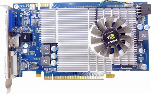
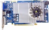
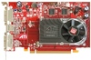
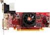
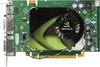
NVIDIA GeForce 9600 GS

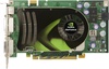
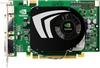
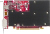
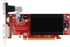
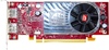
NVIDIA GeForce 9500 GT
|
48 Shaders
768MB DDR2
500MHz
|
32 Shaders
512MB GDDR3
550MHz
|
|
Peak AI Performance
0.12 TOPS
INT32
|
Peak AI Performance
0.09 TOPS
INT32
|
|
FP32
120 GFLOPS
|
FP32
90 GFLOPS
|
|
-
-
|
-
-
|
|
Form Factor
PCIe Card
1.0-Slots
|
Form Factor
PCIe Card
1.0-Slots
|
|
TDP
Unknown
|
TDP
50W
|
|
Power Connectors
1x 6-Pin
-
-
-
|
-
-
-
-
-
|
|
GB6 OpenCL N/A
0%
|
GB6 OpenCL N/A
0%
|
|
GB6 Metal N/A
0%
|
GB6 Metal N/A
0%
|
|
GB6 Vulkan N/A
0%
|
GB6 Vulkan N/A
0%
|
|
GB5 OpenCL N/A
0%
|
GB5 OpenCL N/A
0%
|
|
GB5 CUDA N/A
0%
|
GB5 CUDA N/A
0%
|
|
GB5 Metal N/A
0%
|
GB5 Metal N/A
0%
|
|
GB5 Vulkan N/A
0%
|
GB5 Vulkan N/A
0%
|
|
OCT 2020.1 N/A
0%
|
OCT 2020.1 N/A
0%
|
|
OCT Metal N/A
0%
|
OCT Metal N/A
0%
|
|
Peak AI
Performance
0.12 TOPS
INT32
|
Peak AI
Performance
0.09 TOPS
INT32
|
|
-
-
-
|
-
-
-
|
|
-
-
-
-
-
-
|
-
-
-
-
-
-
|
|
-
-
-
-
-
-
|
-
-
-
-
-
-
|
|
FP32
120 GFLOPS
-
-
|
FP32
90 GFLOPS
-
-
|
|
-
-
-
|
-
-
-
|
|
-
-
-
-
|
-
-
-
-
|
|
-
-
-
|
-
-
-
|
|
-
-
-
|
-
-
-
|
|
-
-
-
-
|
-
-
-
-
|
|
INT32
0.12 TOPS
|
INT32
0.09 TOPS
|
|
-
-
|
-
-
|
|
Pixel
Fillrate
6 GPixel/s
|
Pixel
Fillrate
4.4 GPixel/s
|
|
-
-
|
-
-
|
|
Texture
Fillrate
12 GTexel/s
|
Texture
Fillrate
8.8 GTexel/s
|
|
Manufacturer
NVIDIA
|
Manufacturer
NVIDIA
|
|
Chip Designer
NVIDIA
|
Chip Designer
NVIDIA
|
|
Architecture
Tesla
|
Architecture
Tesla
|
|
Family
GeForce 9000
|
Family
GeForce 9000
|
|
Codename
NV94
G94
-
-
|
Codename
NV96
G96
Variant
G96-300-C1
|
|
Market Segment
Desktop
|
Market Segment
Desktop
|
|
Release Date
7/29/2008
|
Release Date
7/29/2008
|
|
Foundry
TSMC
-
|
Foundry
UMC
-
|
|
Fabrication Node
65nm
-
|
Fabrication Node
65nm
-
|
|
Die Size
240 mm²
-
|
Die Size
144 mm²
-
|
|
Transistor Count
505 Million
-
|
Transistor Count
314 Million
-
|
|
Transistor Density
2.10M/mm²
-
|
Transistor Density
2.18M/mm²
-
|
|
Form
PCIe Card
|
Form
PCIe Card
|
|
Shading Units
48 Shaders
-
|
Shading Units
32 Shaders
-
|
|
Texture Mapping Units
24 TMUs
|
Texture Mapping Units
16 TMUs
|
|
Render Output Units
12 ROPs
|
Render Output Units
8 ROPs
|
|
-
-
|
-
-
|
|
-
-
|
-
-
|
|
Streaming Multiprocessors
6 SMs
|
Streaming Multiprocessors
4 SMs
|
|
-
-
|
-
-
|
|
-
-
|
-
-
|
|
-
-
|
-
-
|
|
-
1250MHz Shader
-
500MHz
|
-
1400MHz Shader
-
550MHz
|
|
-
-
|
-
-
|
|
L1
-
-
-
Unknown
|
L1
-
-
-
Unknown
|
|
L2
64KB Shared
|
L2
32KB Shared
|
|
-
-
-
|
-
-
-
|
|
768MB
DDR2
-
|
512MB
GDDR3
-
|
|
Bus Width
192Bit
|
Bus Width
128Bit
|
|
Clock
500MHz
Transfer Rate
1GT/s
Bandwidth
24GB/s
|
Clock
800MHz
Transfer Rate
1.6GT/s
Bandwidth
25.6GB/s
|
|
-
-
-
-
-
-
-
-
-
|
-
-
-
-
-
-
-
-
-
|
|
TDP
Unknown
|
TDP
50W
|
|
-
-
|
-
-
|
|
1x VGA
1x S-Video
-
-
-
-
-
-
1x DVI-I Dual-Link
-
-
-
-
-
-
-
-
-
-
-
-
-
-
-
-
-
-
-
-
-
-
-
-
-
-
-
-
-
-
|
-
1x S-Video
-
-
-
-
-
1x DVI-I
1x DVI-I Dual-Link
-
-
-
-
-
-
-
-
-
-
-
-
-
-
-
-
-
-
-
-
-
-
-
-
-
-
-
-
-
-
|
|
Max Resolution
2560x1600
|
Max Resolution
2560x1600
|
|
Max Resolution Refresh Rate
60Hz
|
Max Resolution Refresh Rate
60Hz
|
|
Variable Refresh Rate
-
-
-
|
Variable Refresh Rate
-
-
-
|
|
Display Stream Compression (DSC)
Not Supported
|
Display Stream Compression (DSC)
Not Supported
|
|
Multi Monitor Support
2
|
Multi Monitor Support
2
|
|
-
-
|
-
-
|
|
No Encoders
-
|
No Encoders
-
|
|
-
-
-
-
-
-
-
-
-
-
-
-
-
-
-
|
-
-
-
-
-
-
-
-
-
-
-
-
-
-
-
|
|
No Decoders
|
No Decoders
|
|
-
-
-
-
-
-
-
-
-
-
-
-
-
-
|
-
-
-
-
-
-
-
-
-
-
-
-
-
-
|
|
Direct X
11
Direct 3D
10_0
|
Direct X
11
Direct 3D
10_0
|
|
OpenGL
3.3
OpenCL
1.1
-
-
|
OpenGL
3.3
OpenCL
1.1
-
-
|
|
Shader Model
4.0
CUDA
1.1
-
-
PureVideo HD
VP2
VDPAU
Feature Set A
|
Shader Model
4.0
CUDA
1.1
-
-
PureVideo HD
VP3
VDPAU
Feature Set B
|
|
-
-
-
1x Fan
|
-
-
-
1x Fan
|
|
Power Connectors
-
-
1x 6-Pin
-
-
-
-
|
-
-
-
-
-
-
-
-
|
|
Slots Required
1.0
PCIe Version
2.0
PCIe Lanes
16
|
Slots Required
1.0
PCIe Version
2.0
PCIe Lanes
16
|
|
Multi GPU Support
Supported
Type
2-way SLI
|
Multi GPU Support
Supported
Type
2-way SLI
|
|
-
-
-
-
-
-
|
-
-
-
-
-
-
|


Copy Link