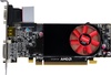
NVIDIA GeForce GTS 150 vs NVIDIA GeForce GT 440 3SM
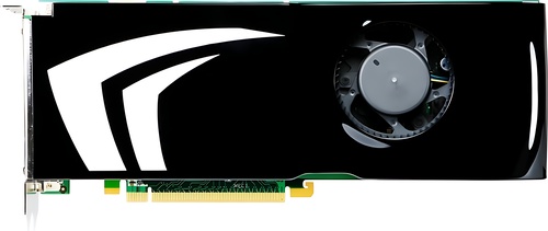
NVIDIA GeForce GTS 150
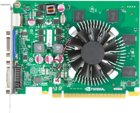
NVIDIA GeForce GT 440 3SM
|
128 Shaders
1GB GDDR3
738MHz
|
144 Shaders
2GB DDR3
810MHz
|
|
Peak AI Performance
0.47 TOPS
INT32
|
Peak AI Performance
0.47 TOPS
INT32
|
|
FP32
470 GFLOPS
|
FP32
470 GFLOPS
|
|
-
-
|
-
-
|
|
Form Factor
PCIe Card
2.0-Slots
|
Form Factor
PCIe Card
1.0-Slots
|
|
TDP
141W
|
TDP
56W
|
|
-
-
-
-
-
|
-
-
-
-
-
|
|
GB6 OpenCL N/A
0%
|
GB6 OpenCL N/A
0%
|
|
GB6 Metal N/A
0%
|
GB6 Metal N/A
0%
|
|
GB6 Vulkan N/A
0%
|
GB6 Vulkan N/A
0%
|
|
GB5 OpenCL N/A
0%
|
GB5 OpenCL N/A
0%
|
|
GB5 CUDA N/A
0%
|
GB5 CUDA N/A
0%
|
|
GB5 Metal N/A
0%
|
GB5 Metal N/A
0%
|
|
GB5 Vulkan N/A
0%
|
GB5 Vulkan N/A
0%
|
|
OCT 2020.1 N/A
0%
|
OCT 2020.1 N/A
0%
|
|
OCT Metal N/A
0%
|
OCT Metal N/A
0%
|
|
Peak AI
Performance
0.47 TOPS
INT32
|
Peak AI
Performance
0.47 TOPS
INT32
|
|
-
-
-
|
-
-
-
|
|
-
-
-
-
-
-
|
-
-
-
-
-
-
|
|
-
-
-
-
-
-
|
-
-
-
-
-
-
|
|
FP32
470 GFLOPS
-
-
|
FP32
470 GFLOPS
-
-
|
|
-
-
-
|
FP64
40 GFLOPS
-
|
|
-
-
-
-
|
-
-
-
-
|
|
-
-
-
|
-
-
-
|
|
-
-
-
|
-
-
-
|
|
-
-
-
-
|
-
-
-
-
|
|
INT32
0.47 TOPS
|
INT32
0.47 TOPS
|
|
-
-
|
-
-
|
|
Pixel
Fillrate
11.808 GPixel/s
|
Pixel
Fillrate
19.44 GPixel/s
|
|
-
-
|
-
-
|
|
Texture
Fillrate
47.232 GTexel/s
|
Texture
Fillrate
19.44 GTexel/s
|
|
Manufacturer
NVIDIA
|
Manufacturer
NVIDIA
|
|
Chip Designer
NVIDIA
|
Chip Designer
NVIDIA
|
|
Architecture
Tesla
|
Architecture
Fermi
|
|
Family
GeForce 100
|
Family
GeForce 400
|
|
Codename
NV92
G92B
-
-
|
Codename
NVC3
GF106
-
-
|
|
Market Segment
Desktop
|
Market Segment
Desktop
|
|
Release Date
3/10/2009
|
Release Date
10/11/2010
|
|
Foundry
TSMC
-
|
Foundry
TSMC
-
|
|
Fabrication Node
55nm
-
|
Fabrication Node
40nm
-
|
|
Die Size
260 mm²
-
|
Die Size
238 mm²
-
|
|
Transistor Count
754 Million
-
|
Transistor Count
1.2 Billion
-
|
|
Transistor Density
2.90M/mm²
-
|
Transistor Density
4.92M/mm²
-
|
|
Form
PCIe Card
|
Form
PCIe Card
|
|
Shading Units
128 Shaders
-
|
Shading Units
144 Shaders
-
|
|
Texture Mapping Units
64 TMUs
|
Texture Mapping Units
24 TMUs
|
|
Render Output Units
16 ROPs
|
Render Output Units
24 ROPs
|
|
-
-
|
-
-
|
|
-
-
|
-
-
|
|
Streaming Multiprocessors
16 SMs
|
Streaming Multiprocessors
3 SMs
|
|
-
-
|
-
-
|
|
-
-
|
-
-
|
|
-
-
|
-
-
|
|
-
1836MHz Shader
-
738MHz
|
-
1620MHz Shader
-
810MHz
|
|
-
-
|
-
-
|
|
L1
-
-
-
Unknown
|
L1
-
64KB/SM
-
-
|
|
L2
64KB Shared
|
L2
384KB Shared
|
|
-
-
-
|
-
-
-
|
|
1GB
GDDR3
-
|
2GB
DDR3
-
|
|
Bus Width
256Bit
|
Bus Width
192Bit
|
|
Clock
1000MHz
Transfer Rate
2GT/s
Bandwidth
64GB/s
|
Clock
900MHz
Transfer Rate
1.8GT/s
Bandwidth
43.2GB/s
|
|
-
-
-
-
-
-
-
-
-
|
-
-
-
-
-
-
-
-
-
|
|
TDP
141W
|
TDP
56W
|
|
-
-
|
-
-
|
|
-
1x S-Video
-
-
-
-
-
-
2x DVI-I Dual-Link
-
-
-
-
-
-
-
-
-
-
-
-
-
-
-
-
-
-
-
-
-
-
-
-
-
-
-
-
-
-
|
1x VGA
-
-
-
-
-
-
-
1x DVI-I Dual-Link
-
-
-
-
-
-
-
-
-
-
-
-
-
-
-
-
-
-
-
-
-
-
-
-
1x HDMI 1.3
-
-
-
-
-
|
|
Max Resolution
2560x1600
|
Max Resolution
2560x1600
|
|
Max Resolution Refresh Rate
60Hz
|
Max Resolution Refresh Rate
60Hz
|
|
Variable Refresh Rate
-
-
-
|
Variable Refresh Rate
-
-
-
|
|
Display Stream Compression (DSC)
Not Supported
|
Display Stream Compression (DSC)
Not Supported
|
|
Multi Monitor Support
2
|
Multi Monitor Support
2
|
|
-
-
|
-
-
|
|
No Encoders
-
|
No Encoders
-
|
|
-
-
-
-
-
-
-
-
-
-
-
-
-
-
-
|
-
-
-
-
-
-
-
-
-
-
-
-
-
-
-
|
|
No Decoders
|
No Decoders
|
|
-
-
-
-
-
-
-
-
-
-
-
-
-
-
|
-
-
-
-
-
-
-
-
-
-
-
-
-
-
|
|
Direct X
11
Direct 3D
10_0
|
Direct X
12
Direct 3D
11_0
|
|
OpenGL
3.3
OpenCL
1.1
-
-
|
OpenGL
4.6
OpenCL
1.1
-
-
|
|
Shader Model
4.0
CUDA
1.1
-
-
PureVideo HD
VP2
VDPAU
Feature Set A
|
Shader Model
5.1
CUDA
2.1
-
-
PureVideo HD
VP4
VDPAU
Feature Set C
|
|
-
-
-
1x Fan
|
-
-
-
1x Fan
|
|
-
-
-
-
-
-
-
-
|
-
-
-
-
-
-
-
-
|
|
Slots Required
2.0
PCIe Version
2.0
PCIe Lanes
16
|
Slots Required
1.0
PCIe Version
2.0
PCIe Lanes
16
|
|
Multi GPU Support
Supported
Type
2-way SLI
|
Multi GPU Support
Supported
Type
3-way SLI
|
|
Height
111 mm (4.37 in)
Width
267 mm (10.51 in)
Depth
38 mm (1.5 in)
|
Height
111 mm (4.37 in)
Width
145 mm (5.71 in)
Depth
20 mm (0.79 in)
|


Copy Link