NVIDIA GeForce GTX 1050 Ti vs AMD Radeon RX 560DX
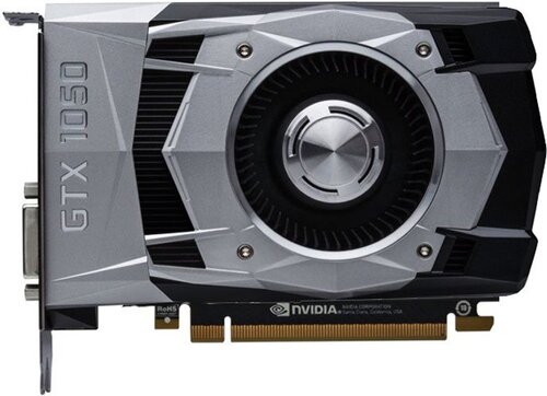
NVIDIA GeForce GTX 1050 Ti
$139
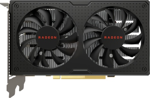
AMD Radeon RX 560DX
|
768 Shaders
4GB GDDR5
1392MHz
|
896 Shaders
4GB GDDR5
1175MHz
|
|
Peak AI Performance
8.55 TOPS
INT8
|
Peak AI Performance
2.11 TFLOPS
FP16
|
|
FP32
2.14 TFLOPS
|
FP32
2.11 TFLOPS
|
|
FP16
30 GFLOPS
|
FP16
2.11 TFLOPS
|
|
Form Factor
PCIe Card
2.0-Slots
|
Form Factor
PCIe Card
2.0-Slots
|
|
TDP
75W
|
TDP
65W
|
|
-
-
-
-
-
|
-
-
-
-
-
|
|
GB6 OpenCL N/A
0%
|
|
|
GB6 Metal N/A
0%
|
GB6 Metal N/A
0%
|
|
GB6 Vulkan N/A
0%
|
|
GB5 OpenCL N/A
0%
|
GB5 OpenCL N/A
0%
|
|
GB5 CUDA N/A
0%
|
GB5 CUDA N/A
0%
|
|
GB5 Metal N/A
0%
|
GB5 Metal N/A
0%
|
|
GB5 Vulkan N/A
0%
|
GB5 Vulkan N/A
0%
|
|
OCT 2020.1 N/A
0%
|
OCT 2020.1 N/A
0%
|
|
OCT Metal N/A
0%
|
OCT Metal N/A
0%
|
|
Peak AI
Performance
8.55 TOPS
INT8
|
Peak AI
Performance
2.11 TFLOPS
FP16
|
|
-
-
-
|
-
-
-
|
|
-
-
-
-
-
-
|
-
-
-
-
-
-
|
|
FP16
30 GFLOPS
-
-
-
-
|
FP16
2.11 TFLOPS
-
-
-
-
|
|
FP32
2.14 TFLOPS
-
-
|
FP32
2.11 TFLOPS
-
-
|
|
FP64
70 GFLOPS
-
|
FP64
130 GFLOPS
-
|
|
-
-
-
-
|
-
-
-
-
|
|
-
-
-
|
-
-
-
|
|
-
-
-
|
-
-
-
|
|
INT8
8.55 TOPS
-
-
|
-
-
-
-
|
|
-
-
|
-
-
|
|
-
-
|
-
-
|
|
Pixel
Fillrate
44.544 GPixel/s
|
Pixel
Fillrate
18.8 GPixel/s
|
|
-
-
|
-
-
|
|
Texture
Fillrate
66.816 GTexel/s
|
Texture
Fillrate
65.8 GTexel/s
|
|
Manufacturer
NVIDIA
|
Manufacturer
AMD
|
|
Chip Designer
NVIDIA
|
Chip Designer
AMD
|
|
Architecture
Pascal
|
Architecture
GCN 4
|
|
Family
GeForce 10
|
Family
Radeon RX 500
|
|
Codename
NV137
GP107
Variant
GP107-400-A1
|
Codename
Baffin
Polaris 21
Variant
Polaris 21 XL
|
|
Market Segment
Desktop
|
Market Segment
Desktop
|
|
Release Date
10/25/2016
|
Release Date
4/11/2018
|
|
Foundry
Samsung
-
|
Foundry
GlobalFoundries
-
|
|
Fabrication Node
14LPP
-
|
Fabrication Node
14LPP
-
|
|
Die Size
132 mm²
-
|
Die Size
123 mm²
-
|
|
Transistor Count
3.3 Billion
-
|
Transistor Count
3 Billion
-
|
|
Transistor Density
25.00M/mm²
-
|
Transistor Density
24.39M/mm²
-
|
|
Form
PCIe Card
|
Form
PCIe Card
|
|
Shading Units
768 Shaders
-
|
Shading Units
896 Shaders
-
|
|
Texture Mapping Units
48 TMUs
|
Texture Mapping Units
56 TMUs
|
|
Render Output Units
32 ROPs
|
Render Output Units
16 ROPs
|
|
-
-
|
-
-
|
|
-
-
|
-
-
|
|
Streaming Multiprocessors
6 SMs
|
-
-
|
|
-
-
|
Compute Units
14 CUs
|
|
-
-
|
-
-
|
|
Graphics Processing Clusters
2 GPCs
|
-
-
|
|
-
-
1290MHz Base
1392MHz
|
-
-
1090MHz Base
1175MHz
|
|
-
-
|
-
-
|
|
L1
-
48KB/SM
-
-
|
L1
-
-
16KB/CU
-
|
|
L2
1MB Shared
|
L2
1MB Shared
|
|
-
-
-
|
-
-
-
|
|
4GB
GDDR5
-
|
4GB
GDDR5
-
|
|
Bus Width
128Bit
|
Bus Width
128Bit
|
|
Clock
1750MHz
Transfer Rate
7GT/s
Bandwidth
112GB/s
|
Clock
1500MHz
Transfer Rate
6GT/s
Bandwidth
96GB/s
|
|
-
-
-
-
-
-
-
-
-
|
-
-
-
-
-
-
-
-
-
|
|
TDP
75W
|
TDP
65W
|
|
-
-
|
-
-
|
|
-
-
-
-
-
-
-
-
-
-
1x DVI-D Dual-Link
-
-
-
-
-
-
-
-
-
-
-
-
-
1x DisplayPort 1.4
-
-
-
-
-
-
-
-
-
-
1x HDMI 2.0
-
-
-
|
-
-
-
-
-
-
-
-
-
-
1x DVI-D Dual-Link
-
-
-
-
-
-
-
-
-
-
-
-
-
1x DisplayPort 1.4
-
-
-
-
-
-
-
-
-
-
1x HDMI 2.0
-
-
-
|
|
Max Resolution
7680x4320
|
Max Resolution
5120x2880
|
|
Max Resolution Refresh Rate
30Hz
|
Max Resolution Refresh Rate
60Hz
|
|
Variable Refresh Rate
G-Sync
FreeSync
-
|
Variable Refresh Rate
-
FreeSync
-
|
|
Display Stream Compression (DSC)
Not Supported
|
Display Stream Compression (DSC)
Not Supported
|
|
Multi Monitor Support
3
|
Multi Monitor Support
3
|
|
-
-
|
Content Protection
HDCP 2.2
|
|
Model
NVENC 4
|
Model
VCE 3.4
|
|
Codec
-
-
-
-
-
-
-
-
AVC (H.264)
HEVC (H.265)
-
-
-
-
|
Codec
-
-
-
-
-
-
-
-
AVC (H.264)
HEVC (H.265)
-
-
-
-
|
|
Model
NVDEC 3
|
Model
UVD 6.3
|
|
Codec
MPEG-1
MPEG-2
MPEG-4
-
VC-1
-
VP9
-
AVC (H.264)
HEVC (H.265)
-
-
-
-
|
Codec
MPEG-1
MPEG-2
MPEG-4
JPEG
VC-1
-
-
-
AVC (H.264)
HEVC (H.265)
-
-
-
-
|
|
Direct X
12
Direct 3D
12_1
|
Direct X
12
Direct 3D
12_0
|
|
OpenGL
4.6
OpenCL
3.0
Vulkan
1.3
|
OpenGL
4.6
OpenCL
2.1
Vulkan
1.3
|
|
Shader Model
6.7
CUDA
6.1
-
-
PureVideo HD
VP8
VDPAU
Feature Set H
|
Shader Model
6.7
-
-
GFX
8
-
-
-
-
|
|
-
-
-
1x Fan
|
-
-
-
2x Fans
|
|
-
-
-
-
-
-
-
-
|
-
-
-
-
-
-
-
-
|
|
Slots Required
2.0
PCIe Version
3.0
PCIe Lanes
16
|
Slots Required
2.0
PCIe Version
3.0
PCIe Lanes
8
|
|
-
-
-
-
|
Multi GPU Support
Supported
Type
CrossFire XDMA
|
|
Height
112 mm (4.41 in)
Width
155 mm (6.1 in)
Depth
40 mm (1.57 in)
|
Height
110 mm (4.33 in)
Width
170 mm (6.69 in)
Depth
37 mm (1.46 in)
|


Copy Link