NVIDIA GeForce GTX 275 vs ATI Radeon HD 5570
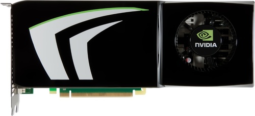
NVIDIA GeForce GTX 275
$250
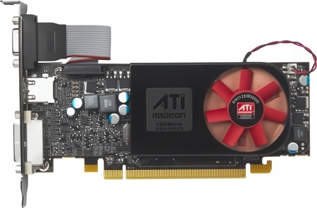
ATI Radeon HD 5570
$80
|
240 Shaders
896MB GDDR3
633MHz
|
400 Shaders
512MB GDDR3
650MHz
|
|
Peak AI Performance
0.67 TOPS
INT32
|
Peak AI Performance
520 GFLOPS
FP32
|
|
FP32
670 GFLOPS
|
FP32
520 GFLOPS
|
|
-
-
|
-
-
|
|
Form Factor
PCIe Card
2.0-Slots
|
Form Factor
PCIe Card
1.0-Slots
|
|
TDP
219W
|
TDP
39W
|
|
Power Connectors
2x 6-Pin
-
-
-
|
-
-
-
-
-
|
|
GB6 OpenCL N/A
0%
|
|
|
GB6 Metal N/A
0%
|
GB6 Metal N/A
0%
|
|
GB6 Vulkan N/A
0%
|
GB6 Vulkan N/A
0%
|
|
GB5 OpenCL N/A
0%
|
GB5 OpenCL N/A
0%
|
|
GB5 CUDA N/A
0%
|
GB5 CUDA N/A
0%
|
|
GB5 Metal N/A
0%
|
GB5 Metal N/A
0%
|
|
GB5 Vulkan N/A
0%
|
GB5 Vulkan N/A
0%
|
|
OCT 2020.1 N/A
0%
|
OCT 2020.1 N/A
0%
|
|
OCT Metal N/A
0%
|
OCT Metal N/A
0%
|
|
Peak AI
Performance
0.67 TOPS
INT32
|
Peak AI
Performance
520 GFLOPS
FP32
|
|
-
-
-
|
-
-
-
|
|
-
-
-
-
-
-
|
-
-
-
-
-
-
|
|
-
-
-
-
-
-
|
-
-
-
-
-
-
|
|
FP32
670 GFLOPS
-
-
|
FP32
520 GFLOPS
-
-
|
|
FP64
80 GFLOPS
-
|
-
-
-
|
|
-
-
-
-
|
-
-
-
-
|
|
-
-
-
|
-
-
-
|
|
-
-
-
|
-
-
-
|
|
-
-
-
-
|
-
-
-
-
|
|
INT32
0.67 TOPS
|
-
-
|
|
-
-
|
-
-
|
|
Pixel
Fillrate
17.724 GPixel/s
|
Pixel
Fillrate
5.2 GPixel/s
|
|
-
-
|
-
-
|
|
Texture
Fillrate
50.64 GTexel/s
|
Texture
Fillrate
13 GTexel/s
|
|
Manufacturer
NVIDIA
|
Manufacturer
ATI
|
|
Chip Designer
NVIDIA
|
Chip Designer
ATI
|
|
Architecture
Tesla 2
|
Architecture
TeraScale 2
|
|
Family
GeForce 200
|
Family
Radeon HD 5000
|
|
Codename
NVA0
GT200B
Variant
GT200-105-B3
|
Codename
Redwood
RV830
Variant
Redwood Pro
|
|
Market Segment
Desktop
|
Market Segment
Desktop
|
|
Release Date
4/9/2009
|
Release Date
2/9/2010
|
|
Foundry
TSMC
-
|
Foundry
TSMC
-
|
|
Fabrication Node
55nm
-
|
Fabrication Node
40nm
-
|
|
Die Size
470 mm²
-
|
Die Size
104 mm²
-
|
|
Transistor Count
1.4 Billion
-
|
Transistor Count
627 Million
-
|
|
Transistor Density
2.98M/mm²
-
|
Transistor Density
6.03M/mm²
-
|
|
Form
PCIe Card
|
Form
PCIe Card
|
|
Shading Units
240 Shaders
-
|
Shading Units
400 Shaders
-
|
|
Texture Mapping Units
80 TMUs
|
Texture Mapping Units
20 TMUs
|
|
Render Output Units
28 ROPs
|
Render Output Units
8 ROPs
|
|
-
-
|
-
-
|
|
-
-
|
-
-
|
|
Streaming Multiprocessors
30 SMs
|
-
-
|
|
-
-
|
Compute Units
5 CUs
|
|
-
-
|
-
-
|
|
-
-
|
-
-
|
|
-
1404MHz Shader
-
633MHz
|
-
-
-
650MHz
|
|
-
-
|
-
-
|
|
L1
-
-
-
Unknown
|
L1
-
-
8KB/CU
-
|
|
L2
256KB Shared
|
L2
256KB Shared
|
|
-
-
-
|
-
-
-
|
|
896MB
GDDR3
-
|
512MB
GDDR3
-
|
|
Bus Width
448Bit
|
Bus Width
128Bit
|
|
Clock
1134MHz
Transfer Rate
2.3GT/s
Bandwidth
127GB/s
|
Clock
800MHz
Transfer Rate
1.6GT/s
Bandwidth
25.6GB/s
|
|
-
-
-
-
-
-
-
-
-
|
-
-
-
-
-
-
-
-
-
|
|
TDP
219W
|
TDP
39W
|
|
-
-
|
-
-
|
|
-
-
-
-
-
-
-
-
2x DVI-I Dual-Link
-
-
-
-
-
-
-
-
-
-
-
-
-
-
-
-
-
-
-
-
-
-
-
-
-
-
-
-
-
-
|
1x VGA
-
-
-
-
-
-
-
1x DVI-I Dual-Link
-
-
-
-
-
-
-
-
-
-
-
-
-
-
-
-
-
-
-
-
-
-
-
-
1x HDMI 1.3
-
-
-
-
-
|
|
Max Resolution
2560x1600
|
Max Resolution
2560x1600
|
|
Max Resolution Refresh Rate
60Hz
|
Max Resolution Refresh Rate
60Hz
|
|
Variable Refresh Rate
-
-
-
|
Variable Refresh Rate
-
-
-
|
|
Display Stream Compression (DSC)
Not Supported
|
Display Stream Compression (DSC)
Not Supported
|
|
Multi Monitor Support
2
|
Multi Monitor Support
2
|
|
-
-
|
-
-
|
|
No Encoders
-
|
No Encoders
-
|
|
-
-
-
-
-
-
-
-
-
-
-
-
-
-
-
|
-
-
-
-
-
-
-
-
-
-
-
-
-
-
-
|
|
No Decoders
|
Model
UVD 2.2
|
|
-
-
-
-
-
-
-
-
-
-
-
-
-
-
|
Codec
-
-
-
-
VC-1
-
-
-
AVC (H.264)
-
-
-
-
-
|
|
Direct X
11
Direct 3D
10_0
|
Direct X
11
Direct 3D
11_0
|
|
OpenGL
3.3
OpenCL
1.1
-
-
|
OpenGL
4.5
OpenCL
1.2
-
-
|
|
Shader Model
4.0
CUDA
1.3
-
-
PureVideo HD
VP2
VDPAU
Feature Set A
|
Shader Model
5.0
-
-
GFX
4
-
-
-
-
|
|
-
-
-
1x Fan
|
-
-
-
1x Fan
|
|
Power Connectors
-
-
2x 6-Pin
-
-
-
-
|
-
-
-
-
-
-
-
-
|
|
Slots Required
2.0
PCIe Version
2.0
PCIe Lanes
16
|
Slots Required
1.0
PCIe Version
2.1
PCIe Lanes
16
|
|
Multi GPU Support
Supported
Type
3-way SLI
|
-
-
-
-
|
|
Height
111 mm (4.37 in)
Width
267 mm (10.51 in)
Depth
38 mm (1.5 in)
|
-
-
-
-
-
-
|


Copy Link