NVIDIA GeForce GTX 480 vs AMD Radeon HD 6770

NVIDIA GeForce GTX 480
$499
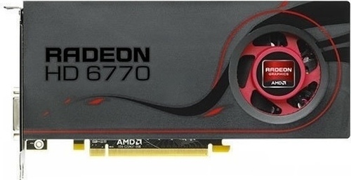
AMD Radeon HD 6770
|
480 Shaders
2GB GDDR5
701MHz
|
800 Shaders
1GB GDDR5
850MHz
|
|
Peak AI Performance
1.35 TOPS
INT32
|
Peak AI Performance
1.36 TFLOPS
FP32
|
|
FP32
1.35 TFLOPS
|
FP32
1.36 TFLOPS
|
|
-
-
|
-
-
|
|
Form Factor
PCIe Card
2.0-Slots
|
Form Factor
PCIe Card
2.0-Slots
|
|
TDP
250W
|
TDP
108W
|
|
Power Connectors
1x 6-Pin
1x 8-Pin
-
-
|
Power Connectors
1x 6-Pin
-
-
-
|
|
GB6 OpenCL N/A
0%
|
|
|
GB6 Metal N/A
0%
|
GB6 Metal N/A
0%
|
|
GB6 Vulkan N/A
0%
|
GB6 Vulkan N/A
0%
|
|
GB5 OpenCL N/A
0%
|
GB5 OpenCL N/A
0%
|
|
GB5 CUDA N/A
0%
|
GB5 CUDA N/A
0%
|
|
GB5 Metal N/A
0%
|
GB5 Metal N/A
0%
|
|
GB5 Vulkan N/A
0%
|
GB5 Vulkan N/A
0%
|
|
OCT 2020.1 N/A
0%
|
OCT 2020.1 N/A
0%
|
|
OCT Metal N/A
0%
|
OCT Metal N/A
0%
|
|
Peak AI
Performance
1.35 TOPS
INT32
|
Peak AI
Performance
1.36 TFLOPS
FP32
|
|
-
-
-
|
-
-
-
|
|
-
-
-
-
-
-
|
-
-
-
-
-
-
|
|
-
-
-
-
-
-
|
-
-
-
-
-
-
|
|
FP32
1.35 TFLOPS
-
-
|
FP32
1.36 TFLOPS
-
-
|
|
FP64
170 GFLOPS
-
|
-
-
-
|
|
-
-
-
-
|
-
-
-
-
|
|
-
-
-
|
-
-
-
|
|
-
-
-
|
-
-
-
|
|
-
-
-
-
|
-
-
-
-
|
|
INT32
1.35 TOPS
|
-
-
|
|
-
-
|
-
-
|
|
Pixel
Fillrate
33.648 GPixel/s
|
Pixel
Fillrate
13.6 GPixel/s
|
|
-
-
|
-
-
|
|
Texture
Fillrate
42.06 GTexel/s
|
Texture
Fillrate
34 GTexel/s
|
|
Manufacturer
NVIDIA
|
Manufacturer
AMD
|
|
Chip Designer
NVIDIA
|
Chip Designer
AMD
|
|
Architecture
Fermi
|
Architecture
TeraScale 2
|
|
Family
GeForce 400
|
Family
Radeon HD 6000
|
|
Codename
NVC0
GF100
Variant
GF100-375-A3
|
Codename
Juniper
RV840
Variant
Juniper XT
|
|
Market Segment
Desktop
|
Market Segment
Desktop
|
|
Release Date
3/26/2010
|
Release Date
4/19/2011
|
|
Foundry
TSMC
-
|
Foundry
TSMC
-
|
|
Fabrication Node
40nm
-
|
Fabrication Node
40nm
-
|
|
Die Size
529 mm²
-
|
Die Size
166 mm²
-
|
|
Transistor Count
3 Billion
-
|
Transistor Count
1 Billion
-
|
|
Transistor Density
5.67M/mm²
-
|
Transistor Density
6.27M/mm²
-
|
|
Form
PCIe Card
|
Form
PCIe Card
|
|
Shading Units
480 Shaders
-
|
Shading Units
800 Shaders
-
|
|
Texture Mapping Units
60 TMUs
|
Texture Mapping Units
40 TMUs
|
|
Render Output Units
48 ROPs
|
Render Output Units
16 ROPs
|
|
-
-
|
-
-
|
|
-
-
|
-
-
|
|
Streaming Multiprocessors
15 SMs
|
-
-
|
|
-
-
|
Compute Units
10 CUs
|
|
-
-
|
-
-
|
|
-
-
|
-
-
|
|
-
1401MHz Shader
-
701MHz
|
-
-
-
850MHz
|
|
-
-
|
-
-
|
|
L1
-
64KB/SM
-
-
|
L1
-
-
8KB/CU
-
|
|
L2
768KB Shared
|
L2
256KB Shared
|
|
-
-
-
|
-
-
-
|
|
2GB
GDDR5
-
|
1GB
GDDR5
-
|
|
Bus Width
384Bit
|
Bus Width
128Bit
|
|
Clock
924MHz
Transfer Rate
3.7GT/s
Bandwidth
177.4GB/s
|
Clock
1200MHz
Transfer Rate
4.8GT/s
Bandwidth
76.8GB/s
|
|
-
-
-
-
-
-
-
-
-
|
-
-
-
-
-
-
-
-
-
|
|
TDP
250W
|
TDP
108W
|
|
-
-
|
-
-
|
|
-
-
-
-
-
-
-
-
2x DVI-I Dual-Link
-
-
-
-
-
-
-
-
-
-
-
-
-
-
-
-
-
-
1x mini-HDMI 1.3
-
-
-
-
-
-
-
-
-
-
-
|
-
-
-
-
-
-
-
-
2x DVI-I Dual-Link
-
-
-
-
-
-
-
-
-
-
-
-
1x DisplayPort 1.1
-
-
-
-
-
-
-
-
-
-
-
1x HDMI 1.3
-
-
-
-
-
|
|
Max Resolution
2560x1600
|
Max Resolution
2560x1600
|
|
Max Resolution Refresh Rate
60Hz
|
Max Resolution Refresh Rate
60Hz
|
|
Variable Refresh Rate
-
-
-
|
Variable Refresh Rate
-
-
-
|
|
Display Stream Compression (DSC)
Not Supported
|
Display Stream Compression (DSC)
Not Supported
|
|
Multi Monitor Support
2
|
Multi Monitor Support
2
|
|
-
-
|
-
-
|
|
No Encoders
-
|
No Encoders
-
|
|
-
-
-
-
-
-
-
-
-
-
-
-
-
-
-
|
-
-
-
-
-
-
-
-
-
-
-
-
-
-
-
|
|
No Decoders
|
Model
UVD 2.2
|
|
-
-
-
-
-
-
-
-
-
-
-
-
-
-
|
Codec
-
-
-
-
VC-1
-
-
-
AVC (H.264)
-
-
-
-
-
|
|
Direct X
12
Direct 3D
11_0
|
Direct X
11
Direct 3D
11_0
|
|
OpenGL
4.6
OpenCL
1.1
-
-
|
OpenGL
4.5
OpenCL
1.2
-
-
|
|
Shader Model
5.1
CUDA
2.0
-
-
PureVideo HD
VP4
VDPAU
Feature Set C
|
Shader Model
5.0
-
-
GFX
4
-
-
-
-
|
|
-
-
-
1x Fan
|
-
-
-
1x Fan
|
|
Power Connectors
-
-
1x 6-Pin
1x 8-Pin
-
-
-
|
Power Connectors
-
-
1x 6-Pin
-
-
-
-
|
|
Slots Required
2.0
PCIe Version
2.0
PCIe Lanes
16
|
Slots Required
2.0
PCIe Version
2.1
PCIe Lanes
16
|
|
Multi GPU Support
Supported
Type
4-way SLI
|
Multi GPU Support
Supported
Type
4-way CrossFireX
|
|
Height
130 mm (5.12 in)
Width
267 mm (10.51 in)
Depth
38 mm (1.5 in)
|
Height
111 mm (4.37 in)
Width
198 mm (7.8 in)
Depth
36 mm (1.42 in)
|


Copy Link