NVIDIA GeForce GTX 560 vs NVIDIA GeForce GTX 465

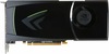
NVIDIA GeForce GTX 560
$199
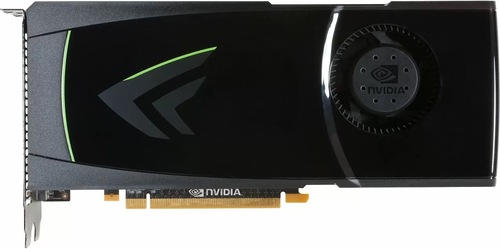
NVIDIA GeForce GTX 465
$279
|
336 Shaders
1GB GDDR5
810MHz
|
352 Shaders
1GB GDDR5
608MHz
|
|
Peak AI Performance
1.09 TOPS
INT32
|
Peak AI Performance
0.86 TOPS
INT32
|
|
FP32
1.09 TFLOPS
|
FP32
860 GFLOPS
|
|
-
-
|
-
-
|
|
Form Factor
PCIe Card
2.0-Slots
|
Form Factor
PCIe Card
2.0-Slots
|
|
TDP
150W
|
TDP
200W
|
|
Power Connectors
2x 6-Pin
-
-
-
|
Power Connectors
2x 6-Pin
-
-
-
|
|
GB6 OpenCL N/A
0%
|
GB6 OpenCL N/A
0%
|
|
GB6 Metal N/A
0%
|
GB6 Metal N/A
0%
|
|
GB6 Vulkan N/A
0%
|
GB6 Vulkan N/A
0%
|
|
GB5 OpenCL N/A
0%
|
GB5 OpenCL N/A
0%
|
|
GB5 CUDA N/A
0%
|
GB5 CUDA N/A
0%
|
|
GB5 Metal N/A
0%
|
GB5 Metal N/A
0%
|
|
GB5 Vulkan N/A
0%
|
GB5 Vulkan N/A
0%
|
|
OCT 2020.1 N/A
0%
|
OCT 2020.1 N/A
0%
|
|
OCT Metal N/A
0%
|
OCT Metal N/A
0%
|
|
Peak AI
Performance
1.09 TOPS
INT32
|
Peak AI
Performance
0.86 TOPS
INT32
|
|
-
-
-
|
-
-
-
|
|
-
-
-
-
-
-
|
-
-
-
-
-
-
|
|
-
-
-
-
-
-
|
-
-
-
-
-
-
|
|
FP32
1.09 TFLOPS
-
-
|
FP32
860 GFLOPS
-
-
|
|
FP64
90 GFLOPS
-
|
FP64
110 GFLOPS
-
|
|
-
-
-
-
|
-
-
-
-
|
|
-
-
-
|
-
-
-
|
|
-
-
-
|
-
-
-
|
|
-
-
-
-
|
-
-
-
-
|
|
INT32
1.09 TOPS
|
INT32
0.86 TOPS
|
|
-
-
|
-
-
|
|
Pixel
Fillrate
25.92 GPixel/s
|
Pixel
Fillrate
19.456 GPixel/s
|
|
-
-
|
-
-
|
|
Texture
Fillrate
45.36 GTexel/s
|
Texture
Fillrate
26.752 GTexel/s
|
|
Manufacturer
NVIDIA
|
Manufacturer
NVIDIA
|
|
Chip Designer
NVIDIA
|
Chip Designer
NVIDIA
|
|
Architecture
Fermi
|
Architecture
Fermi
|
|
Family
GeForce 500
|
Family
GeForce 400
|
|
Codename
NVCE
GF114
Variant
GF114-325-A1
|
Codename
NVC0
GF100
Variant
GF100-030-A3
|
|
Market Segment
Desktop
|
Market Segment
Desktop
|
|
Release Date
5/17/2011
|
Release Date
5/31/2010
|
|
Foundry
TSMC
-
|
Foundry
TSMC
-
|
|
Fabrication Node
40nm
-
|
Fabrication Node
40nm
-
|
|
Die Size
332 mm²
-
|
Die Size
529 mm²
-
|
|
Transistor Count
2 Billion
-
|
Transistor Count
3 Billion
-
|
|
Transistor Density
5.87M/mm²
-
|
Transistor Density
5.67M/mm²
-
|
|
Form
PCIe Card
|
Form
PCIe Card
|
|
Shading Units
336 Shaders
-
|
Shading Units
352 Shaders
-
|
|
Texture Mapping Units
56 TMUs
|
Texture Mapping Units
44 TMUs
|
|
Render Output Units
32 ROPs
|
Render Output Units
32 ROPs
|
|
-
-
|
-
-
|
|
-
-
|
-
-
|
|
Streaming Multiprocessors
7 SMs
|
Streaming Multiprocessors
11 SMs
|
|
-
-
|
-
-
|
|
-
-
|
-
-
|
|
-
-
|
-
-
|
|
-
1620MHz Shader
-
810MHz
|
-
1215MHz Shader
-
608MHz
|
|
-
-
|
-
-
|
|
L1
-
64KB/SM
-
-
|
L1
-
64KB/SM
-
-
|
|
L2
512KB Shared
|
L2
768KB Shared
|
|
-
-
-
|
-
-
-
|
|
1GB
GDDR5
-
|
1GB
GDDR5
-
|
|
Bus Width
256Bit
|
Bus Width
256Bit
|
|
Clock
1002MHz
Transfer Rate
4GT/s
Bandwidth
128.3GB/s
|
Clock
802MHz
Transfer Rate
3.2GT/s
Bandwidth
102.6GB/s
|
|
-
-
-
-
-
-
-
-
-
|
-
-
-
-
-
-
-
-
-
|
|
TDP
150W
|
TDP
200W
|
|
-
-
|
-
-
|
|
-
-
-
-
-
-
-
-
2x DVI-I Dual-Link
-
-
-
-
-
-
-
-
-
-
-
-
-
-
-
-
-
-
1x mini-HDMI 1.3
-
-
-
-
-
-
-
-
-
-
-
|
-
-
-
-
-
-
-
-
2x DVI-I Dual-Link
-
-
-
-
-
-
-
-
-
-
-
-
-
-
-
-
-
-
1x mini-HDMI 1.3
-
-
-
-
-
-
-
-
-
-
-
|
|
Max Resolution
2560x1600
|
Max Resolution
2560x1600
|
|
Max Resolution Refresh Rate
60Hz
|
Max Resolution Refresh Rate
60Hz
|
|
Variable Refresh Rate
-
-
-
|
Variable Refresh Rate
-
-
-
|
|
Display Stream Compression (DSC)
Not Supported
|
Display Stream Compression (DSC)
Not Supported
|
|
Multi Monitor Support
2
|
Multi Monitor Support
2
|
|
-
-
|
-
-
|
|
No Encoders
-
|
No Encoders
-
|
|
-
-
-
-
-
-
-
-
-
-
-
-
-
-
-
|
-
-
-
-
-
-
-
-
-
-
-
-
-
-
-
|
|
No Decoders
|
No Decoders
|
|
-
-
-
-
-
-
-
-
-
-
-
-
-
-
|
-
-
-
-
-
-
-
-
-
-
-
-
-
-
|
|
Direct X
12
Direct 3D
11_0
|
Direct X
12
Direct 3D
11_0
|
|
OpenGL
4.6
OpenCL
1.1
-
-
|
OpenGL
4.6
OpenCL
1.1
-
-
|
|
Shader Model
5.1
CUDA
2.1
-
-
PureVideo HD
VP4
VDPAU
Feature Set C
|
Shader Model
5.1
CUDA
2.0
-
-
PureVideo HD
VP4
VDPAU
Feature Set C
|
|
-
-
-
1x Fan
|
-
-
-
1x Fan
|
|
Power Connectors
-
-
2x 6-Pin
-
-
-
-
|
Power Connectors
-
-
2x 6-Pin
-
-
-
-
|
|
Slots Required
2.0
PCIe Version
2.0
PCIe Lanes
16
|
Slots Required
2.0
PCIe Version
2.0
PCIe Lanes
16
|
|
Multi GPU Support
Supported
Type
2-way SLI
|
Multi GPU Support
Supported
Type
4-way SLI
|
|
Height
111 mm (4.37 in)
Width
210 mm (8.27 in)
Depth
38 mm (1.5 in)
|
Height
111 mm (4.37 in)
Width
241 mm (9.49 in)
Depth
38 mm (1.5 in)
|


Copy Link