NVIDIA GeForce GTX 745 vs NVIDIA GeForce GTX 560 SE
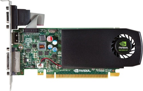
NVIDIA GeForce GTX 745
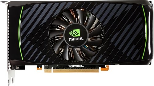
NVIDIA GeForce GTX 560 SE
|
384 Shaders
1GB DDR3
1033MHz
|
288 Shaders
1GB GDDR5
736MHz
|
|
Peak AI Performance
3.17 TOPS
INT8
|
Peak AI Performance
0.85 TOPS
INT32
|
|
FP32
790 GFLOPS
|
FP32
850 GFLOPS
|
|
-
-
|
-
-
|
|
Form Factor
PCIe Card
1.0-Slots
|
Form Factor
PCIe Card
2.0-Slots
|
|
TDP
55W
|
TDP
150W
|
|
-
-
-
-
-
|
Power Connectors
2x 6-Pin
-
-
-
|
|
GB6 OpenCL N/A
0%
|
|
|
GB6 Metal N/A
0%
|
GB6 Metal N/A
0%
|
|
GB6 Vulkan N/A
0%
|
|
GB5 OpenCL N/A
0%
|
GB5 OpenCL N/A
0%
|
|
GB5 CUDA N/A
0%
|
GB5 CUDA N/A
0%
|
|
GB5 Metal N/A
0%
|
GB5 Metal N/A
0%
|
|
GB5 Vulkan N/A
0%
|
GB5 Vulkan N/A
0%
|
|
OCT 2020.1 N/A
0%
|
OCT 2020.1 N/A
0%
|
|
OCT Metal N/A
0%
|
OCT Metal N/A
0%
|
|
Peak AI
Performance
3.17 TOPS
INT8
|
Peak AI
Performance
0.85 TOPS
INT32
|
|
-
-
-
|
-
-
-
|
|
-
-
-
-
-
-
|
-
-
-
-
-
-
|
|
-
-
-
-
-
-
|
-
-
-
-
-
-
|
|
FP32
790 GFLOPS
-
-
|
FP32
850 GFLOPS
-
-
|
|
FP64
30 GFLOPS
-
|
FP64
70 GFLOPS
-
|
|
-
-
-
-
|
-
-
-
-
|
|
-
-
-
|
-
-
-
|
|
-
-
-
|
-
-
-
|
|
INT8
3.17 TOPS
-
-
|
-
-
-
-
|
|
INT32
0.79 TOPS
|
INT32
0.85 TOPS
|
|
-
-
|
-
-
|
|
Pixel
Fillrate
16.528 GPixel/s
|
Pixel
Fillrate
17.664 GPixel/s
|
|
-
-
|
-
-
|
|
Texture
Fillrate
24.792 GTexel/s
|
Texture
Fillrate
35.328 GTexel/s
|
|
Manufacturer
NVIDIA
|
Manufacturer
NVIDIA
|
|
Chip Designer
NVIDIA
|
Chip Designer
NVIDIA
|
|
Architecture
Maxwell
|
Architecture
Fermi
|
|
Family
GeForce 700
|
Family
GeForce 500
|
|
Codename
NV117
GM107
Variant
GM107-220-A2
|
Codename
NVCE
GF114
Variant
GF114-200-KB-A1
|
|
Market Segment
Desktop
|
Market Segment
Desktop
|
|
Release Date
2/18/2014
|
Release Date
2/20/2012
|
|
Foundry
TSMC
-
|
Foundry
TSMC
-
|
|
Fabrication Node
28nm
-
|
Fabrication Node
40nm
-
|
|
Die Size
148 mm²
-
|
Die Size
332 mm²
-
|
|
Transistor Count
1.9 Billion
-
|
Transistor Count
2 Billion
-
|
|
Transistor Density
12.64M/mm²
-
|
Transistor Density
5.87M/mm²
-
|
|
Form
PCIe Card
|
Form
PCIe Card
|
|
Shading Units
384 Shaders
-
|
Shading Units
288 Shaders
-
|
|
Texture Mapping Units
24 TMUs
|
Texture Mapping Units
48 TMUs
|
|
Render Output Units
16 ROPs
|
Render Output Units
24 ROPs
|
|
-
-
|
-
-
|
|
-
-
|
-
-
|
|
Streaming Multiprocessors
3 SMs
|
Streaming Multiprocessors
6 SMs
|
|
-
-
|
-
-
|
|
-
-
|
-
-
|
|
-
-
|
-
-
|
|
-
-
-
1033MHz
|
-
1472MHz Shader
-
736MHz
|
|
-
-
|
-
-
|
|
L1
-
64KB/SM
-
-
|
L1
-
64KB/SM
-
-
|
|
L2
2MB Shared
|
L2
512KB Shared
|
|
-
-
-
|
-
-
-
|
|
1GB
DDR3
-
|
1GB
GDDR5
-
|
|
Bus Width
128Bit
|
Bus Width
128Bit
|
|
Clock
900MHz
Transfer Rate
1.8GT/s
Bandwidth
28.8GB/s
|
Clock
957MHz
Transfer Rate
3.8GT/s
Bandwidth
61.3GB/s
|
|
-
-
-
-
-
-
-
-
-
|
-
-
-
-
-
-
-
-
-
|
|
TDP
55W
|
TDP
150W
|
|
-
-
|
-
-
|
|
1x VGA
-
-
-
-
-
-
-
-
-
1x DVI-D Dual-Link
-
-
-
-
-
-
-
-
-
-
-
-
-
-
-
-
-
-
-
-
-
-
-
1x HDMI 1.4
-
-
-
-
|
-
-
-
-
-
-
-
-
2x DVI-I Dual-Link
-
-
-
-
-
-
-
-
-
-
-
-
-
-
-
-
-
-
1x mini-HDMI 1.3
-
-
-
-
-
-
-
-
-
-
-
|
|
Max Resolution
4096x2304
|
Max Resolution
2560x1600
|
|
Max Resolution Refresh Rate
30Hz
|
Max Resolution Refresh Rate
60Hz
|
|
Variable Refresh Rate
G-Sync
FreeSync
-
|
Variable Refresh Rate
-
-
-
|
|
Display Stream Compression (DSC)
Not Supported
|
Display Stream Compression (DSC)
Not Supported
|
|
Multi Monitor Support
2
|
Multi Monitor Support
2
|
|
-
-
|
-
-
|
|
Model
NVENC 2
|
No Encoders
-
|
|
Codec
-
-
-
-
-
-
-
-
AVC (H.264)
-
-
-
-
-
|
-
-
-
-
-
-
-
-
-
-
-
-
-
-
-
|
|
Model
NVDEC 1
|
No Decoders
|
|
Codec
MPEG-1
MPEG-2
MPEG-4
-
VC-1
-
-
-
AVC (H.264)
-
-
-
-
-
|
-
-
-
-
-
-
-
-
-
-
-
-
-
-
|
|
Direct X
12
Direct 3D
11_0
|
Direct X
12
Direct 3D
11_0
|
|
OpenGL
4.6
OpenCL
3.0
Vulkan
1.3
|
OpenGL
4.6
OpenCL
1.1
-
-
|
|
Shader Model
6.7
CUDA
5.0
-
-
PureVideo HD
VP6
VDPAU
Feature Set E
|
Shader Model
5.1
CUDA
2.1
-
-
PureVideo HD
VP4
VDPAU
Feature Set C
|
|
-
-
-
1x Fan
|
-
-
-
1x Fan
|
|
-
-
-
-
-
-
-
-
|
Power Connectors
-
-
2x 6-Pin
-
-
-
-
|
|
Slots Required
1.0
PCIe Version
3.0
PCIe Lanes
16
|
Slots Required
2.0
PCIe Version
2.0
PCIe Lanes
16
|
|
-
-
-
-
|
Multi GPU Support
Supported
Type
2-way SLI
|
|
Height
69 mm (2.72 in)
Width
155 mm (6.1 in)
Depth
20 mm (0.79 in)
|
Height
111 mm (4.37 in)
Width
210 mm (8.27 in)
Depth
38 mm (1.5 in)
|


Copy Link