NVIDIA GeForce RTX 4070 Super vs EVGA GeForce RTX 3080 10GB FTW3 Ultra
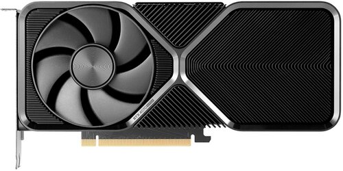
NVIDIA GeForce RTX 4070 Super
$599
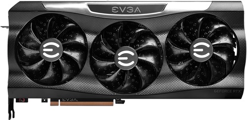
EVGA GeForce RTX 3080 10GB FTW3 Ultra
$770
|
7168 Shaders
12GB GDDR6X
2475MHz
|
8704 Shaders
10GB GDDR6X
1800MHz
|
|
Peak AI Performance
1.14 POPS
INT4 Tensor Sparse
|
Peak AI Performance
1 POPS
INT4 Tensor Sparse
|
|
FP32
35.48 TFLOPS
|
FP32
31.33 TFLOPS
|
|
FP16
35.48 TFLOPS
|
FP16
31.33 TFLOPS
|
|
Form Factor
PCIe Card
2.1-Slots
|
Form Factor
PCIe Card
3.0-Slots
|
|
TDP
225W
|
TDP
320W
|
|
Power Connectors
-
-
-
1x 16-Pin 12VHPWR
|
Power Connectors
-
3x 8-Pin
-
-
|
|
GB6 OpenCL N/A
0%
|
|
|
GB6 Metal N/A
0%
|
GB6 Metal N/A
0%
|
|
GB6 Vulkan N/A
0%
|
|
GB5 OpenCL N/A
0%
|
GB5 OpenCL 190,600
62%
|
|
GB5 CUDA N/A
0%
|
GB5 CUDA 212,430
60%
|
|
GB5 Metal N/A
0%
|
GB5 Metal N/A
0%
|
|
GB5 Vulkan N/A
0%
|
GB5 Vulkan 132,070
64%
|
|
OCT 2020.1 N/A
0%
|
OCT 2020.1 575
76%
|
|
OCT Metal N/A
0%
|
OCT Metal N/A
0%
|
|
Peak AI
Performance
1.14 POPS
INT4 Tensor Sparse
|
Peak AI
Performance
1 POPS
INT4 Tensor Sparse
|
|
-
-
-
|
-
-
-
|
|
FP8
-
283.85 TFLOPS
Tensor (FP16 Accumulate)
567.71 TFLOPS
Tensor (FP16 Accumulate) Sparse
141.93 TFLOPS
Tensor (FP32 Accumulate)
283.85 TFLOPS
Tensor (FP32 Accumulate) Sparse
|
-
-
-
-
-
-
|
|
FP16
35.48 TFLOPS
141.93 TFLOPS
Tensor (FP16 Accumulate)
283.85 TFLOPS
Tensor (FP16 Accumulate) Sparse
70.96 TFLOPS
Tensor (FP32 Accumulate)
141.93 TFLOPS
Tensor (FP32 Accumulate) Sparse
|
FP16
31.33 TFLOPS
125.34 TFLOPS
Tensor (FP16 Accumulate)
250.68 TFLOPS
Tensor (FP16 Accumulate) Sparse
62.67 TFLOPS
Tensor (FP32 Accumulate)
125.34 TFLOPS
Tensor (FP32 Accumulate) Sparse
|
|
FP32
35.48 TFLOPS
-
-
|
FP32
31.33 TFLOPS
-
-
|
|
FP64
550 GFLOPS
-
|
FP64
490 GFLOPS
-
|
|
BF16
35.48 TFLOPS
70.96 TFLOPS
Tensor
141.93 TFLOPS
Tensor Sparse
|
BF16
31.33 TFLOPS
62.67 TFLOPS
Tensor
125.34 TFLOPS
Tensor Sparse
|
|
TF32
35.48 TFLOPS
Tensor
70.96 TFLOPS
Tensor Sparse
|
TF32
31.33 TFLOPS
Tensor
62.67 TFLOPS
Tensor Sparse
|
|
INT4
567.71 TOPS
Tensor
1.14 POPS
Tensor Sparse
|
INT4
501.35 TOPS
Tensor
1 POPS
Tensor Sparse
|
|
INT8
-
283.85 TOPS
Tensor
567.71 TOPS
Tensor Sparse
|
INT8
-
250.68 TOPS
Tensor
501.35 TOPS
Tensor Sparse
|
|
INT32
17.74 TOPS
|
INT32
15.67 TOPS
|
|
Ray Tracing
82 TOPS
|
Ray Tracing
47.3 TOPS
|
|
Pixel
Fillrate
198 GPixel/s
|
Pixel
Fillrate
172.8 GPixel/s
|
|
-
-
|
-
-
|
|
Texture
Fillrate
554.4 GTexel/s
|
Texture
Fillrate
489.6 GTexel/s
|
|
Manufacturer
NVIDIA
|
Manufacturer
EVGA
|
|
Chip Designer
NVIDIA
|
Chip Designer
NVIDIA
|
|
Architecture
Ada Lovelace
|
Architecture
Ampere
|
|
Family
GeForce 40
|
Family
GeForce 30
|
|
Codename
NV184
AD104
Variant
AD104-350-A1
|
Codename
NV172
GA102
Variant
GA102-200-KD-A1
|
|
Market Segment
Desktop
|
Market Segment
Desktop
|
|
Release Date
1/8/2024
|
Release Date
1/27/2022
|
|
Foundry
TSMC
-
|
Foundry
Samsung
-
|
|
Fabrication Node
4N
-
|
Fabrication Node
8N
-
|
|
Die Size
295 mm²
-
|
Die Size
628 mm²
-
|
|
Transistor Count
35.8 Billion
-
|
Transistor Count
28.3 Billion
-
|
|
Transistor Density
121.56M/mm²
-
|
Transistor Density
45.04M/mm²
-
|
|
Form
PCIe Card
|
Form
PCIe Card
|
|
Shading Units
7168 Shaders
-
|
Shading Units
8704 Shaders
-
|
|
Texture Mapping Units
224 TMUs
|
Texture Mapping Units
272 TMUs
|
|
Render Output Units
80 ROPs
|
Render Output Units
96 ROPs
|
|
Tensor Cores
224 T-Cores
|
Tensor Cores
272 T-Cores
|
|
Ray-Tracing Cores
56 RT-Cores
|
Ray-Tracing Cores
68 RT-Cores
|
|
Streaming Multiprocessors
56 SMs
|
Streaming Multiprocessors
68 SMs
|
|
-
-
|
-
-
|
|
-
-
|
-
-
|
|
Graphics Processing Clusters
5 GPCs
|
Graphics Processing Clusters
7 GPCs
|
|
-
-
1980MHz Base
2475MHz
|
-
-
1440MHz Base
1800MHz
|
|
-
-
|
-
-
|
|
L1
64KB/SM Tex
128KB/SM
-
-
|
L1
64KB/SM Tex
128KB/SM
-
-
|
|
L2
36MB Shared
|
L2
5MB Shared
|
|
-
-
-
|
-
-
-
|
|
12GB
GDDR6X
-
|
10GB
GDDR6X
-
|
|
Bus Width
192Bit
|
Bus Width
320Bit
|
|
Clock
1313MHz
Transfer Rate
21GT/s
Bandwidth
504GB/s
|
Clock
1188MHz
Transfer Rate
19GT/s
Bandwidth
760GB/s
|
|
-
-
-
-
-
-
-
-
-
|
-
-
-
-
-
-
-
-
-
|
|
TDP
225W
|
TDP
320W
|
|
-
-
|
Temp
93°C Max
|
|
-
-
-
-
-
-
-
-
-
-
-
-
-
-
-
-
-
-
-
-
-
-
-
-
3x DisplayPort 1.4
-
-
-
-
-
-
-
-
-
-
-
1x HDMI 2.1
-
-
|
-
-
-
-
-
-
-
-
-
-
-
-
-
-
-
-
-
-
-
-
-
-
-
-
3x DisplayPort 1.4
-
-
-
-
-
-
-
-
-
-
-
1x HDMI 2.1
-
-
|
|
Max Resolution
7680x4320
|
Max Resolution
7680x4320
|
|
Max Resolution Refresh Rate
60Hz
|
Max Resolution Refresh Rate
60Hz
|
|
Variable Refresh Rate
G-Sync
FreeSync
-
|
Variable Refresh Rate
G-Sync
FreeSync
-
|
|
Display Stream Compression (DSC)
Supported
|
Display Stream Compression (DSC)
Supported
|
|
Multi Monitor Support
4
|
Multi Monitor Support
4
|
|
Content Protection
HDCP 2.3
|
Content Protection
HDCP 2.3
|
|
Model
2x NVENC 8
|
Model
NVENC 7
|
|
Codec
-
-
-
-
-
-
-
-
AVC (H.264)
HEVC (H.265)
-
AV1
-
-
|
Codec
-
-
-
-
-
-
-
-
AVC (H.264)
HEVC (H.265)
-
-
-
-
|
|
Model
NVDEC 5
|
Model
NVDEC 5
|
|
Codec
MPEG-1
MPEG-2
MPEG-4
-
VC-1
VP8
VP9
-
AVC (H.264)
HEVC (H.265)
-
AV1
-
-
|
Codec
MPEG-1
MPEG-2
MPEG-4
-
VC-1
VP8
VP9
-
AVC (H.264)
HEVC (H.265)
-
AV1
-
-
|
|
Direct X
12
Direct 3D
12_3
|
Direct X
12
Direct 3D
12_2
|
|
OpenGL
4.6
OpenCL
3.0
Vulkan
1.3
|
OpenGL
4.6
OpenCL
3.0
Vulkan
1.2
|
|
Shader Model
6.7
CUDA
8.9
-
-
PureVideo HD
VP12
VDPAU
Feature Set L
|
Shader Model
6.6
CUDA
8.6
-
-
PureVideo HD
VP11
VDPAU
Feature Set K
|
|
-
-
-
2x Fans
|
-
-
-
3x Fans
|
|
Power Connectors
-
-
-
-
-
-
1x 16-Pin 12VHPWR
|
Power Connectors
-
-
-
3x 8-Pin
-
-
-
|
|
Slots Required
2.1
PCIe Version
4.0
PCIe Lanes
16
|
Slots Required
3.0
PCIe Version
4.0
PCIe Lanes
16
|
|
-
-
-
-
|
-
-
-
-
|
|
Height
112 mm (4.41 in)
Width
267 mm (10.51 in)
Depth
42 mm (1.65 in)
|
Height
136.8 mm (5.39 in)
Width
285 mm (11.22 in)
Depth
60 mm (2.36 in)
|


Copy Link