NVIDIA GeForce RTX 4070 Ti vs NVIDIA GeForce RTX 3080 12GB
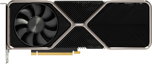
NVIDIA GeForce RTX 4070 Ti
$799
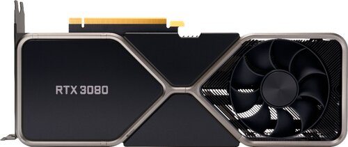
NVIDIA GeForce RTX 3080 12GB
$999
|
7680 Shaders
12GB GDDR6X
2610MHz
|
8960 Shaders
12GB GDDR6X
1710MHz
|
|
Peak AI Performance
1.28 POPS
INT4 Tensor Sparse
|
Peak AI Performance
980.58 TOPS
INT4 Tensor Sparse
|
|
FP32
40.09 TFLOPS
|
FP32
30.64 TFLOPS
|
|
FP16
40.09 TFLOPS
|
FP16
30.64 TFLOPS
|
|
Form Factor
PCIe Card
3.0-Slots
|
Form Factor
PCIe Card
2.0-Slots
|
|
TDP
285W
|
TDP
350W
|
|
Power Connectors
-
-
-
1x 16-Pin 12VHPWR
|
Power Connectors
-
-
1x 12-Pin
-
|
|
GB6 OpenCL N/A
0%
|
|
|
GB6 Metal N/A
0%
|
GB6 Metal N/A
0%
|
|
GB6 Vulkan N/A
0%
|
|
GB5 OpenCL N/A
0%
|
GB5 OpenCL 186,590
61%
|
|
GB5 CUDA N/A
0%
|
GB5 CUDA 207,975
59%
|
|
GB5 Metal N/A
0%
|
GB5 Metal N/A
0%
|
|
GB5 Vulkan N/A
0%
|
GB5 Vulkan 125,525
61%
|
|
OCT 2020.1 N/A
0%
|
OCT 2020.1 595
78%
|
|
OCT Metal N/A
0%
|
OCT Metal N/A
0%
|
|
Peak AI
Performance
1.28 POPS
INT4 Tensor Sparse
|
Peak AI
Performance
980.58 TOPS
INT4 Tensor Sparse
|
|
-
-
-
|
-
-
-
|
|
FP8
-
320.72 TFLOPS
Tensor (FP16 Accumulate)
641.43 TFLOPS
Tensor (FP16 Accumulate) Sparse
160.36 TFLOPS
Tensor (FP32 Accumulate)
320.72 TFLOPS
Tensor (FP32 Accumulate) Sparse
|
-
-
-
-
-
-
|
|
FP16
40.09 TFLOPS
160.36 TFLOPS
Tensor (FP16 Accumulate)
320.72 TFLOPS
Tensor (FP16 Accumulate) Sparse
80.18 TFLOPS
Tensor (FP32 Accumulate)
160.36 TFLOPS
Tensor (FP32 Accumulate) Sparse
|
FP16
30.64 TFLOPS
122.57 TFLOPS
Tensor (FP16 Accumulate)
245.15 TFLOPS
Tensor (FP16 Accumulate) Sparse
61.29 TFLOPS
Tensor (FP32 Accumulate)
122.57 TFLOPS
Tensor (FP32 Accumulate) Sparse
|
|
FP32
40.09 TFLOPS
-
-
|
FP32
30.64 TFLOPS
-
-
|
|
FP64
630 GFLOPS
-
|
FP64
480 GFLOPS
-
|
|
BF16
40.09 TFLOPS
80.18 TFLOPS
Tensor
160.36 TFLOPS
Tensor Sparse
|
BF16
30.64 TFLOPS
61.29 TFLOPS
Tensor
122.57 TFLOPS
Tensor Sparse
|
|
TF32
40.09 TFLOPS
Tensor
80.18 TFLOPS
Tensor Sparse
|
TF32
30.64 TFLOPS
Tensor
61.29 TFLOPS
Tensor Sparse
|
|
INT4
641.43 TOPS
Tensor
1.28 POPS
Tensor Sparse
|
INT4
490.29 TOPS
Tensor
980.58 TOPS
Tensor Sparse
|
|
INT8
-
320.72 TOPS
Tensor
641.43 TOPS
Tensor Sparse
|
INT8
-
245.15 TOPS
Tensor
490.29 TOPS
Tensor Sparse
|
|
INT32
20.05 TOPS
|
INT32
15.32 TOPS
|
|
Ray Tracing
92.7 TOPS
|
Ray Tracing
46.2 TOPS
|
|
Pixel
Fillrate
208.8 GPixel/s
|
Pixel
Fillrate
191.52 GPixel/s
|
|
-
-
|
-
-
|
|
Texture
Fillrate
626.4 GTexel/s
|
Texture
Fillrate
478.8 GTexel/s
|
|
Manufacturer
NVIDIA
|
Manufacturer
NVIDIA
|
|
Chip Designer
NVIDIA
|
Chip Designer
NVIDIA
|
|
Architecture
Ada Lovelace
|
Architecture
Ampere
|
|
Family
GeForce 40
|
Family
GeForce 30
|
|
Codename
NV184
AD104
Variant
AD104-400-A1
|
Codename
NV172
GA102
Variant
GA102-220-A1
|
|
Market Segment
Desktop
|
Market Segment
Desktop
|
|
Release Date
1/5/2023
|
Release Date
1/27/2022
|
|
Foundry
TSMC
-
|
Foundry
Samsung
-
|
|
Fabrication Node
4N
-
|
Fabrication Node
8N
-
|
|
Die Size
295 mm²
-
|
Die Size
628 mm²
-
|
|
Transistor Count
35.8 Billion
-
|
Transistor Count
28.3 Billion
-
|
|
Transistor Density
121.56M/mm²
-
|
Transistor Density
45.04M/mm²
-
|
|
Form
PCIe Card
|
Form
PCIe Card
|
|
Shading Units
7680 Shaders
-
|
Shading Units
8960 Shaders
-
|
|
Texture Mapping Units
240 TMUs
|
Texture Mapping Units
280 TMUs
|
|
Render Output Units
80 ROPs
|
Render Output Units
112 ROPs
|
|
Tensor Cores
240 T-Cores
|
Tensor Cores
280 T-Cores
|
|
Ray-Tracing Cores
60 RT-Cores
|
Ray-Tracing Cores
70 RT-Cores
|
|
Streaming Multiprocessors
60 SMs
|
Streaming Multiprocessors
70 SMs
|
|
-
-
|
-
-
|
|
-
-
|
-
-
|
|
Graphics Processing Clusters
5 GPCs
|
Graphics Processing Clusters
7 GPCs
|
|
-
-
2310MHz Base
2610MHz
|
-
-
1260MHz Base
1710MHz
|
|
-
-
|
-
-
|
|
L1
64KB/SM Tex
128KB/SM
-
-
|
L1
64KB/SM Tex
128KB/SM
-
-
|
|
L2
48MB Shared
|
L2
5MB Shared
|
|
-
-
-
|
-
-
-
|
|
12GB
GDDR6X
-
|
12GB
GDDR6X
-
|
|
Bus Width
192Bit
|
Bus Width
384Bit
|
|
Clock
1313MHz
Transfer Rate
21GT/s
Bandwidth
504GB/s
|
Clock
1188MHz
Transfer Rate
19GT/s
Bandwidth
912GB/s
|
|
-
-
-
-
-
-
-
-
-
|
-
-
-
-
-
-
-
-
-
|
|
TDP
285W
|
TDP
350W
|
|
Temp
90°C Max
|
Temp
93°C Max
|
|
-
-
-
-
-
-
-
-
-
-
-
-
-
-
-
-
-
-
-
-
-
-
-
-
3x DisplayPort 1.4
-
-
-
-
-
-
-
-
-
-
-
1x HDMI 2.1
-
-
|
-
-
-
-
-
-
-
-
-
-
-
-
-
-
-
-
-
-
-
-
-
-
-
-
3x DisplayPort 1.4
-
-
-
-
-
-
-
-
-
-
-
1x HDMI 2.1
-
-
|
|
Max Resolution
7680x4320
|
Max Resolution
7680x4320
|
|
Max Resolution Refresh Rate
60Hz
|
Max Resolution Refresh Rate
60Hz
|
|
Variable Refresh Rate
G-Sync
FreeSync
-
|
Variable Refresh Rate
G-Sync
FreeSync
-
|
|
Display Stream Compression (DSC)
Supported
|
Display Stream Compression (DSC)
Supported
|
|
Multi Monitor Support
4
|
Multi Monitor Support
4
|
|
Content Protection
HDCP 2.3
|
Content Protection
HDCP 2.3
|
|
Model
2x NVENC 8
|
Model
NVENC 7
|
|
Codec
-
-
-
-
-
-
-
-
AVC (H.264)
HEVC (H.265)
-
AV1
-
-
|
Codec
-
-
-
-
-
-
-
-
AVC (H.264)
HEVC (H.265)
-
-
-
-
|
|
Model
NVDEC 5
|
Model
NVDEC 5
|
|
Codec
MPEG-1
MPEG-2
MPEG-4
-
VC-1
VP8
VP9
-
AVC (H.264)
HEVC (H.265)
-
AV1
-
-
|
Codec
MPEG-1
MPEG-2
MPEG-4
-
VC-1
VP8
VP9
-
AVC (H.264)
HEVC (H.265)
-
AV1
-
-
|
|
Direct X
12
Direct 3D
12_3
|
Direct X
12
Direct 3D
12_2
|
|
OpenGL
4.6
OpenCL
3.0
Vulkan
1.3
|
OpenGL
4.6
OpenCL
3.0
Vulkan
1.2
|
|
Shader Model
6.6
CUDA
8.9
-
-
PureVideo HD
VP12
VDPAU
Feature Set L
|
Shader Model
6.6
CUDA
8.6
-
-
PureVideo HD
VP11
VDPAU
Feature Set K
|
|
-
-
-
2x Fans
|
-
-
-
2x Fans
|
|
Power Connectors
-
-
-
-
-
-
1x 16-Pin 12VHPWR
|
Power Connectors
-
-
-
-
-
1x 12-Pin
-
|
|
Slots Required
3.0
PCIe Version
4.0
PCIe Lanes
16
|
Slots Required
2.0
PCIe Version
4.0
PCIe Lanes
16
|
|
-
-
-
-
|
-
-
-
-
|
|
Height
137 mm (5.39 in)
Width
304 mm (11.97 in)
Depth
61 mm (2.4 in)
|
Height
112 mm (4.41 in)
Width
285 mm (11.22 in)
Depth
40 mm (1.57 in)
|


Copy Link