NVIDIA Quadro FX 4700 X2 vs ATI FireGL V7600
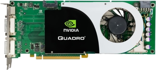
NVIDIA Quadro FX 4700 X2
$2,999
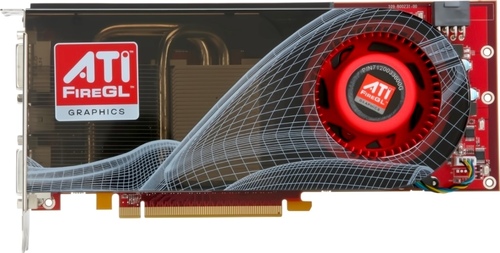
ATI FireGL V7600
$999
|
2x 128 Shaders
2GB (2x 1GB) GDDR3
600MHz
|
240 Shaders
512MB GDDR3
600MHz
|
|
Peak AI Performance
0.77 TOPS
INT32
|
Peak AI Performance
290 GFLOPS
FP32
|
|
FP32
770 GFLOPS
|
FP32
290 GFLOPS
|
|
-
-
|
-
-
|
|
Form Factor
PCIe Card
2.0-Slots
|
Form Factor
PCIe Card
2.0-Slots
|
|
TDP
226W
|
TDP
127W
|
|
Power Connectors
1x 6-Pin
1x 8-Pin
-
-
|
Power Connectors
-
1x 8-Pin
-
-
|
|
GB6 OpenCL N/A
0%
|
GB6 OpenCL N/A
0%
|
|
GB6 Metal N/A
0%
|
GB6 Metal N/A
0%
|
|
GB6 Vulkan N/A
0%
|
GB6 Vulkan N/A
0%
|
|
GB5 OpenCL N/A
0%
|
GB5 OpenCL N/A
0%
|
|
GB5 CUDA N/A
0%
|
GB5 CUDA N/A
0%
|
|
GB5 Metal N/A
0%
|
GB5 Metal N/A
0%
|
|
GB5 Vulkan N/A
0%
|
GB5 Vulkan N/A
0%
|
|
OCT 2020.1 N/A
0%
|
OCT 2020.1 N/A
0%
|
|
OCT Metal N/A
0%
|
OCT Metal N/A
0%
|
|
Peak AI
Performance
0.77 TOPS
INT32
|
Peak AI
Performance
290 GFLOPS
FP32
|
|
-
-
-
|
-
-
-
|
|
-
-
-
-
-
-
|
-
-
-
-
-
-
|
|
-
-
-
-
-
-
|
-
-
-
-
-
-
|
|
FP32
770 GFLOPS
-
-
|
FP32
290 GFLOPS
-
-
|
|
-
-
-
|
-
-
-
|
|
-
-
-
-
|
-
-
-
-
|
|
-
-
-
|
-
-
-
|
|
-
-
-
|
-
-
-
|
|
-
-
-
-
|
-
-
-
-
|
|
INT32
0.77 TOPS
|
-
-
|
|
-
-
|
-
-
|
|
Pixel
Fillrate
9.6 GPixel/s
|
Pixel
Fillrate
7.2 GPixel/s
|
|
-
-
|
-
-
|
|
Texture
Fillrate
38.4 GTexel/s
|
Texture
Fillrate
7.2 GTexel/s
|
|
Manufacturer
NVIDIA
|
Manufacturer
ATI
|
|
Chip Designer
NVIDIA
|
Chip Designer
ATI
|
|
Architecture
Tesla
|
Architecture
TeraScale 1
|
|
Family
Quadro FX7
|
Family
FireGL V
|
|
Codename
NV92
G92
Variant
G92-880-A2
|
Codename
Pele
R600
Variant
R600 GL
|
|
Market Segment
Workstation
|
Market Segment
Workstation
|
|
Release Date
4/18/2008
|
Release Date
8/6/2007
|
|
Foundry
TSMC
-
|
Foundry
TSMC
-
|
|
Fabrication Node
65nm
-
|
Fabrication Node
90nm
-
|
|
Die Size
2x 324 mm²
-
|
Die Size
352 mm²
-
|
|
Transistor Count
2x 754 Million
-
|
Transistor Count
384 Million
-
|
|
Transistor Density
2.33M/mm²
-
|
Transistor Density
1.09M/mm²
-
|
|
Form
PCIe Card
|
Form
PCIe Card
|
|
Shading Units
2x 128 Shaders
-
|
Shading Units
240 Shaders
-
|
|
Texture Mapping Units
2x 64 TMUs
|
Texture Mapping Units
12 TMUs
|
|
Render Output Units
2x 16 ROPs
|
Render Output Units
12 ROPs
|
|
-
-
|
-
-
|
|
-
-
|
-
-
|
|
Streaming Multiprocessors
2x 16 SMs
|
-
-
|
|
-
-
|
Compute Units
3 CUs
|
|
-
-
|
-
-
|
|
-
-
|
-
-
|
|
-
1500MHz Shader
-
600MHz
|
-
-
-
600MHz
|
|
-
-
|
-
-
|
|
L1
-
-
-
Unknown
|
L1
-
-
-
Unknown
|
|
L2
64KB Shared
|
L2
Unknown
|
|
-
-
-
|
-
-
-
|
|
2GB (2x 1GB)
GDDR3
-
|
512MB
GDDR3
-
|
|
Bus Width
256Bit
|
Bus Width
256Bit
|
|
Clock
800MHz
Transfer Rate
1.6GT/s
Bandwidth
51.2GB/s
|
Clock
800MHz
Transfer Rate
1.6GT/s
Bandwidth
51.2GB/s
|
|
-
-
-
-
-
-
-
-
-
|
-
-
-
-
-
-
-
-
-
|
|
TDP
226W
|
TDP
127W
|
|
-
-
|
-
-
|
|
-
-
-
-
1x SDI
-
-
-
4x DVI-I Dual-Link
-
-
-
-
-
-
-
-
-
-
-
-
-
-
-
-
-
-
-
-
-
-
-
-
-
-
-
-
-
-
|
-
1x S-Video
-
-
-
-
-
-
2x DVI-I Dual-Link
-
-
-
-
-
-
-
-
-
-
-
-
-
-
-
-
-
-
-
-
-
-
-
-
-
-
-
-
-
-
|
|
Max Resolution
2560x1600
|
Max Resolution
2560x1600
|
|
Max Resolution Refresh Rate
60Hz
|
Max Resolution Refresh Rate
60Hz
|
|
Variable Refresh Rate
-
-
-
|
Variable Refresh Rate
-
-
-
|
|
Display Stream Compression (DSC)
Not Supported
|
Display Stream Compression (DSC)
Not Supported
|
|
Multi Monitor Support
4
|
Multi Monitor Support
2
|
|
-
-
|
-
-
|
|
No Encoders
-
|
No Encoders
-
|
|
-
-
-
-
-
-
-
-
-
-
-
-
-
-
-
|
-
-
-
-
-
-
-
-
-
-
-
-
-
-
-
|
|
No Decoders
|
No Decoders
|
|
-
-
-
-
-
-
-
-
-
-
-
-
-
-
|
-
-
-
-
-
-
-
-
-
-
-
-
-
-
|
|
Direct X
11
Direct 3D
10_0
|
Direct X
9
Direct 3D
9_3
|
|
OpenGL
3.3
OpenCL
1.1
-
-
|
OpenGL
2.1
-
-
-
-
|
|
Shader Model
4.0
CUDA
1.1
-
-
PureVideo HD
VP2
VDPAU
Feature Set A
|
Shader Model
3.0
-
-
GFX
2
-
-
-
-
|
|
-
-
-
1x Fan
|
-
-
-
1x Fan
|
|
Power Connectors
-
-
1x 6-Pin
1x 8-Pin
-
-
-
|
Power Connectors
-
-
-
1x 8-Pin
-
-
-
|
|
Slots Required
2.0
PCIe Version
2.0
PCIe Lanes
16
|
Slots Required
2.0
PCIe Version
2.0
PCIe Lanes
16
|
|
Multi GPU Support
Supported
Type
2-way SLI
|
Multi GPU Support
Supported
Type
4-way CrossFireX
|
|
Height
111 mm (4.37 in)
Width
267 mm (10.51 in)
Depth
39 mm (1.54 in)
|
Height
111 mm (4.37 in)
Width
254 mm (10 in)
Depth
37 mm (1.46 in)
|


Copy Link