NVIDIA Tesla M2070Q vs NVIDIA GRID K340

NVIDIA Tesla M2070Q
$5,489
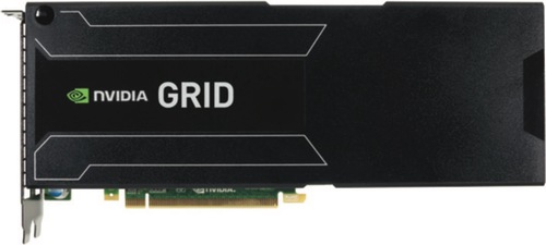
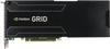
NVIDIA GRID K340
$3,299
|
448 Shaders
6GB GDDR5
575MHz
|
4x 384 Shaders
4GB (4x 1GB) GDDR5
954MHz
|
|
Peak AI Performance
1.03 TOPS
INT32
|
Peak AI Performance
2.93 TOPS
INT32
|
|
FP32
1.03 TFLOPS
|
FP32
2.93 TFLOPS
|
|
-
-
|
-
-
|
|
Form Factor
PCIe Card
2.0-Slots
|
Form Factor
PCIe Card
2.0-Slots
|
|
TDP
225W
|
TDP
225W
|
|
Power Connectors
1x 6-Pin
1x 8-Pin
-
-
|
Power Connectors
-
1x 8-Pin
-
-
|
|
GB6 OpenCL N/A
0%
|
GB6 OpenCL N/A
0%
|
|
GB6 Metal N/A
0%
|
GB6 Metal N/A
0%
|
|
GB6 Vulkan N/A
0%
|
GB6 Vulkan N/A
0%
|
|
GB5 OpenCL N/A
0%
|
GB5 OpenCL N/A
0%
|
|
GB5 CUDA N/A
0%
|
GB5 CUDA N/A
0%
|
|
GB5 Metal N/A
0%
|
GB5 Metal N/A
0%
|
|
GB5 Vulkan N/A
0%
|
GB5 Vulkan N/A
0%
|
|
OCT 2020.1 N/A
0%
|
OCT 2020.1 N/A
0%
|
|
OCT Metal N/A
0%
|
OCT Metal N/A
0%
|
|
Peak AI
Performance
1.03 TOPS
INT32
|
Peak AI
Performance
2.93 TOPS
INT32
|
|
-
-
-
|
-
-
-
|
|
-
-
-
-
-
-
|
-
-
-
-
-
-
|
|
-
-
-
-
-
-
|
-
-
-
-
-
-
|
|
FP32
1.03 TFLOPS
-
-
|
FP32
2.93 TFLOPS
-
-
|
|
FP64
130 GFLOPS
-
|
FP64
120 GFLOPS
-
|
|
-
-
-
-
|
-
-
-
-
|
|
-
-
-
|
-
-
-
|
|
-
-
-
|
-
-
-
|
|
-
-
-
-
|
-
-
-
-
|
|
INT32
1.03 TOPS
|
INT32
2.93 TOPS
|
|
-
-
|
-
-
|
|
Pixel
Fillrate
27.6 GPixel/s
|
Pixel
Fillrate
15.264 GPixel/s
|
|
-
-
|
-
-
|
|
Texture
Fillrate
32.2 GTexel/s
|
Texture
Fillrate
30.528 GTexel/s
|
|
Manufacturer
NVIDIA
|
Manufacturer
NVIDIA
|
|
Chip Designer
NVIDIA
|
Chip Designer
NVIDIA
|
|
Architecture
Fermi
|
Architecture
Kepler
|
|
Family
Tesla 20
|
Family
GRID
|
|
Codename
NVC0
GF100
Variant
GF100-876-A1
|
Codename
NVE7
GK107
-
-
|
|
Market Segment
Server
|
Market Segment
Server
|
|
Release Date
7/25/2011
|
Release Date
7/23/2013
|
|
Foundry
TSMC
-
|
Foundry
TSMC
-
|
|
Fabrication Node
40nm
-
|
Fabrication Node
28nm
-
|
|
Die Size
3000 mm²
-
|
Die Size
4x 118 mm²
-
|
|
Transistor Count
529 Million
-
|
Transistor Count
4x 1.3 Billion
-
|
|
Transistor Density
0.18M/mm²
-
|
Transistor Density
10.76M/mm²
-
|
|
Form
PCIe Card
|
Form
PCIe Card
|
|
Shading Units
448 Shaders
-
|
Shading Units
4x 384 Shaders
-
|
|
Texture Mapping Units
56 TMUs
|
Texture Mapping Units
4x 32 TMUs
|
|
Render Output Units
48 ROPs
|
Render Output Units
4x 16 ROPs
|
|
-
-
|
-
-
|
|
-
-
|
-
-
|
|
Streaming Multiprocessors
14 SMs
|
Streaming Multiprocessors
4x 2 SMs
|
|
-
-
|
-
-
|
|
-
-
|
-
-
|
|
-
-
|
-
-
|
|
-
1150MHz Shader
-
575MHz
|
-
-
-
954MHz
|
|
-
-
|
-
-
|
|
L1
-
64KB/SM
-
-
|
L1
48KB/SM Tex
16KB/SM
-
-
|
|
L2
768KB Shared
|
L2
256KB Shared
|
|
-
-
-
|
-
-
-
|
|
6GB
GDDR5
-
|
4GB (4x 1GB)
GDDR5
-
|
|
Bus Width
384Bit
|
Bus Width
128Bit
|
|
Clock
783MHz
Transfer Rate
3.1GT/s
Bandwidth
150.3GB/s
|
Clock
1250MHz
Transfer Rate
5GT/s
Bandwidth
80GB/s
|
|
-
-
-
-
-
-
-
-
-
|
-
-
-
-
-
-
-
-
-
|
|
TDP
225W
|
TDP
225W
|
|
-
-
|
-
-
|
|
-
-
-
-
-
-
-
-
-
-
-
-
-
-
-
-
-
-
-
-
-
-
-
-
-
-
-
-
-
-
-
-
-
-
-
-
-
-
-
No Ports
|
-
-
-
-
-
-
-
-
-
-
-
-
-
-
-
-
-
-
-
-
-
-
-
-
-
-
-
-
-
-
-
-
-
-
-
-
-
-
-
No Ports
|
|
Max Resolution
Unknown
|
Max Resolution
Unknown
|
|
Max Resolution Refresh Rate
-
|
Max Resolution Refresh Rate
-
|
|
Variable Refresh Rate
-
-
-
|
Variable Refresh Rate
G-Sync
FreeSync
-
|
|
Display Stream Compression (DSC)
Not Supported
|
Display Stream Compression (DSC)
Not Supported
|
|
Multi Monitor Support
Unknown
|
Multi Monitor Support
Unknown
|
|
-
-
|
-
-
|
|
No Encoders
-
|
Model
NVENC 1
|
|
-
-
-
-
-
-
-
-
-
-
-
-
-
-
-
|
Codec
-
-
-
-
-
-
-
-
AVC (H.264)
-
-
-
-
-
|
|
No Decoders
|
Model
NVDEC 1
|
|
-
-
-
-
-
-
-
-
-
-
-
-
-
-
|
Codec
MPEG-1
MPEG-2
MPEG-4
-
VC-1
-
-
-
AVC (H.264)
-
-
-
-
-
|
|
Direct X
12
Direct 3D
11_0
|
Direct X
12
Direct 3D
11_0
|
|
OpenGL
4.6
OpenCL
1.1
-
-
|
OpenGL
4.6
OpenCL
3.0
Vulkan
1.2
|
|
Shader Model
5.1
CUDA
2.0
-
-
PureVideo HD
VP4
VDPAU
Feature Set C
|
Shader Model
6.5
CUDA
3.0
-
-
PureVideo HD
VP5
VDPAU
Feature Set D
|
|
-
-
-
-
|
-
-
-
-
|
|
Power Connectors
-
-
1x 6-Pin
1x 8-Pin
-
-
-
|
Power Connectors
-
-
-
1x 8-Pin
-
-
-
|
|
Slots Required
2.0
PCIe Version
2.0
PCIe Lanes
16
|
Slots Required
2.0
PCIe Version
3.0
PCIe Lanes
16
|
|
Multi GPU Support
Supported
-
-
|
-
-
-
-
|
|
Height
111 mm (4.37 in)
Width
248 mm (9.76 in)
Depth
39 mm (1.54 in)
|
Height
111 mm (4.37 in)
Width
267 mm (10.51 in)
Depth
40 mm (1.57 in)
|


Copy Link