NVIDIA Tesla M60 vs AMD FirePro S9100
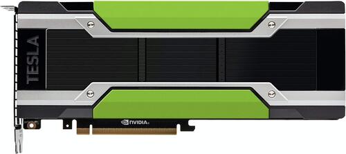
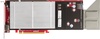
NVIDIA Tesla M60
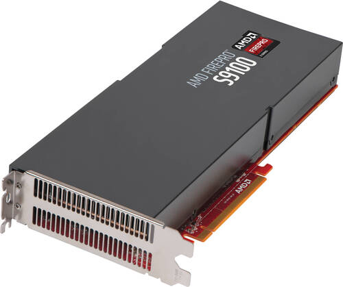
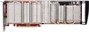
AMD FirePro S9100
|
2x 2048 Shaders
16GB (2x 8GB) GDDR5
1178MHz
|
2560 Shaders
12GB GDDR5
824MHz
|
|
Peak AI Performance
38.6 TOPS
INT8
|
Peak AI Performance
4.22 TFLOPS
FP32
|
|
FP32
9.65 TFLOPS
|
FP32
4.22 TFLOPS
|
|
-
-
|
-
-
|
|
Form Factor
PCIe Card
2.0-Slots
|
Form Factor
PCIe Card
2.0-Slots
|
|
TDP
300W
|
TDP
225W
|
|
Power Connectors
-
1x 8-Pin
-
-
|
Power Connectors
1x 6-Pin
1x 8-Pin
-
-
|
|
GB6 OpenCL N/A
0%
|
GB6 OpenCL N/A
0%
|
|
GB6 Metal N/A
0%
|
GB6 Metal N/A
0%
|
|
GB6 Vulkan N/A
0%
|
GB6 Vulkan N/A
0%
|
|
GB5 OpenCL N/A
0%
|
GB5 OpenCL N/A
0%
|
|
GB5 CUDA N/A
0%
|
GB5 CUDA N/A
0%
|
|
GB5 Metal N/A
0%
|
GB5 Metal N/A
0%
|
|
GB5 Vulkan N/A
0%
|
GB5 Vulkan N/A
0%
|
|
OCT 2020.1 N/A
0%
|
OCT 2020.1 N/A
0%
|
|
OCT Metal N/A
0%
|
OCT Metal N/A
0%
|
|
Peak AI
Performance
38.6 TOPS
INT8
|
Peak AI
Performance
4.22 TFLOPS
FP32
|
|
-
-
-
|
-
-
-
|
|
-
-
-
-
-
-
|
-
-
-
-
-
-
|
|
-
-
-
-
-
-
|
-
-
-
-
-
-
|
|
FP32
9.65 TFLOPS
-
-
|
FP32
4.22 TFLOPS
-
-
|
|
FP64
300 GFLOPS
-
|
FP64
2.11 TFLOPS
-
|
|
-
-
-
-
|
-
-
-
-
|
|
-
-
-
|
-
-
-
|
|
-
-
-
|
-
-
-
|
|
INT8
38.6 TOPS
-
-
|
-
-
-
-
|
|
INT32
9.65 TOPS
|
-
-
|
|
-
-
|
-
-
|
|
Pixel
Fillrate
75.392 GPixel/s
|
Pixel
Fillrate
52.736 GPixel/s
|
|
-
-
|
-
-
|
|
Texture
Fillrate
150.784 GTexel/s
|
Texture
Fillrate
131.84 GTexel/s
|
|
Manufacturer
NVIDIA
|
Manufacturer
AMD
|
|
Chip Designer
NVIDIA
|
Chip Designer
AMD
|
|
Architecture
Maxwell 2
|
Architecture
GCN 2
|
|
Family
Tesla M
|
Family
FirePro S
|
|
Codename
NV124
GM204
-
-
|
Codename
Hawaii
-
Variant
Hawaii Pro GL
|
|
Market Segment
Server
|
Market Segment
Server
|
|
Release Date
8/30/2015
|
Release Date
10/2/2014
|
|
Foundry
TSMC
-
|
Foundry
TSMC
-
|
|
Fabrication Node
28nm
-
|
Fabrication Node
28nm
-
|
|
Die Size
2x 398 mm²
-
|
Die Size
438 mm²
-
|
|
Transistor Count
2x 5.2 Billion
-
|
Transistor Count
6.2 Billion
-
|
|
Transistor Density
13.07M/mm²
-
|
Transistor Density
14.16M/mm²
-
|
|
Form
PCIe Card
|
Form
PCIe Card
|
|
Shading Units
2x 2048 Shaders
-
|
Shading Units
2560 Shaders
-
|
|
Texture Mapping Units
2x 128 TMUs
|
Texture Mapping Units
160 TMUs
|
|
Render Output Units
2x 64 ROPs
|
Render Output Units
64 ROPs
|
|
-
-
|
-
-
|
|
-
-
|
-
-
|
|
Streaming Multiprocessors
2x 16 SMs
|
-
-
|
|
-
-
|
Compute Units
40 CUs
|
|
-
-
|
-
-
|
|
-
-
|
-
-
|
|
-
-
899MHz Base
1178MHz
|
-
-
-
824MHz
|
|
-
-
|
-
-
|
|
L1
-
48KB/SM
-
-
|
L1
-
-
16KB/CU
-
|
|
L2
2MB Shared
|
L2
1MB Shared
|
|
-
-
-
|
-
-
-
|
|
16GB (2x 8GB)
GDDR5
-
|
12GB
GDDR5
-
|
|
Bus Width
256Bit
|
Bus Width
512Bit
|
|
Clock
1250MHz
Transfer Rate
5GT/s
Bandwidth
160GB/s
|
Clock
1250MHz
Transfer Rate
5GT/s
Bandwidth
320GB/s
|
|
-
-
-
-
-
-
-
-
-
|
-
-
-
-
-
-
-
-
-
|
|
TDP
300W
|
TDP
225W
|
|
-
-
|
-
-
|
|
-
-
-
-
-
-
-
-
-
-
-
-
-
-
-
-
-
-
-
-
-
-
-
-
-
-
-
-
-
-
-
-
-
-
-
-
-
-
-
No Ports
|
-
-
-
-
-
-
-
-
-
-
-
-
-
-
-
-
-
-
-
-
-
-
-
-
-
-
-
-
-
-
-
-
-
-
-
-
-
-
-
No Ports
|
|
Max Resolution
Unknown
|
Max Resolution
4096x2160
|
|
Max Resolution Refresh Rate
-
|
Max Resolution Refresh Rate
60Hz
|
|
Variable Refresh Rate
G-Sync
FreeSync
-
|
Variable Refresh Rate
-
FreeSync
-
|
|
Display Stream Compression (DSC)
Not Supported
|
Display Stream Compression (DSC)
Not Supported
|
|
Multi Monitor Support
Unknown
|
Multi Monitor Support
3
|
|
-
-
|
Content Protection
HDCP 1.4
|
|
Model
2x NVENC 3
|
Model
VCE 2.0
|
|
Codec
-
-
-
-
-
-
-
-
AVC (H.264)
HEVC (H.265)
-
-
-
-
|
Codec
-
-
-
-
-
-
-
-
AVC (H.264)
-
-
-
-
-
|
|
Model
NVDEC 1
|
Model
UVD 4.2
|
|
Codec
MPEG-1
MPEG-2
MPEG-4
-
VC-1
-
-
-
AVC (H.264)
-
-
-
-
-
|
Codec
MPEG-1
MPEG-2
MPEG-4
-
VC-1
-
-
-
AVC (H.264)
-
-
-
-
-
|
|
Direct X
12
Direct 3D
12_1
|
Direct X
12
Direct 3D
12_0
|
|
OpenGL
4.6
OpenCL
3.0
Vulkan
1.3
|
OpenGL
4.6
OpenCL
2.1
Vulkan
1.2
|
|
Shader Model
6.7
CUDA
5.2
-
-
PureVideo HD
VP6
VDPAU
Feature Set E
|
Shader Model
6.5
-
-
GFX
7
-
-
-
-
|
|
-
-
-
-
|
-
-
-
-
|
|
Power Connectors
-
-
-
1x 8-Pin
-
-
-
|
Power Connectors
-
-
1x 6-Pin
1x 8-Pin
-
-
-
|
|
Slots Required
2.0
PCIe Version
3.0
PCIe Lanes
16
|
Slots Required
2.0
PCIe Version
3.0
PCIe Lanes
16
|
|
-
-
-
-
|
Multi GPU Support
Supported
Type
CrossFire XDMA
|
|
Height
111 mm (4.37 in)
Width
267 mm (10.51 in)
Depth
40 mm (1.57 in)
|
Height
111 mm (4.37 in)
Width
267 mm (10.51 in)
Depth
37 mm (1.46 in)
|


Copy Link