NVIDIA Tesla Quadro Plex 2200 S4 vs NVIDIA Tesla S1070-500

NVIDIA Tesla Quadro Plex 2200 S4
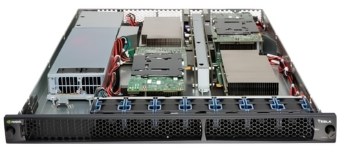
NVIDIA Tesla S1070-500
$7,999
|
4x 240 Shaders
16GB (4x 4GB) GDDR3
648MHz
|
4x 240 Shaders
16GB (4x 4GB) GDDR3
602MHz
|
|
Peak AI Performance
2.49 TOPS
INT32
|
Peak AI Performance
2.49 TOPS
INT32
|
|
FP32
2.49 TFLOPS
|
FP32
2.49 TFLOPS
|
|
-
-
|
-
-
|
|
Form Factor
1U
-
|
Form Factor
1U
-
|
|
TDP
1200W
|
TDP
800W
|
|
-
-
-
-
-
|
-
-
-
-
-
|
|
GB6 OpenCL N/A
0%
|
GB6 OpenCL N/A
0%
|
|
GB6 Metal N/A
0%
|
GB6 Metal N/A
0%
|
|
GB6 Vulkan N/A
0%
|
GB6 Vulkan N/A
0%
|
|
GB5 OpenCL N/A
0%
|
GB5 OpenCL N/A
0%
|
|
GB5 CUDA N/A
0%
|
GB5 CUDA N/A
0%
|
|
GB5 Metal N/A
0%
|
GB5 Metal N/A
0%
|
|
GB5 Vulkan N/A
0%
|
GB5 Vulkan N/A
0%
|
|
OCT 2020.1 N/A
0%
|
OCT 2020.1 N/A
0%
|
|
OCT Metal N/A
0%
|
OCT Metal N/A
0%
|
|
Peak AI
Performance
2.49 TOPS
INT32
|
Peak AI
Performance
2.49 TOPS
INT32
|
|
-
-
-
|
-
-
-
|
|
-
-
-
-
-
-
|
-
-
-
-
-
-
|
|
-
-
-
-
-
-
|
-
-
-
-
-
-
|
|
FP32
2.49 TFLOPS
-
-
|
FP32
2.49 TFLOPS
-
-
|
|
FP64
310 GFLOPS
-
|
FP64
310 GFLOPS
-
|
|
-
-
-
-
|
-
-
-
-
|
|
-
-
-
|
-
-
-
|
|
-
-
-
|
-
-
-
|
|
-
-
-
-
|
-
-
-
-
|
|
INT32
2.49 TOPS
|
INT32
2.49 TOPS
|
|
-
-
|
-
-
|
|
Pixel
Fillrate
20.736 GPixel/s
|
Pixel
Fillrate
19.264 GPixel/s
|
|
-
-
|
-
-
|
|
Texture
Fillrate
51.84 GTexel/s
|
Texture
Fillrate
48.16 GTexel/s
|
|
Foundry
TSMC
-
|
Foundry
TSMC
-
|
|
Fabrication Node
55nm
-
|
Fabrication Node
55nm
-
|
|
Die Size
4x 470 mm²
-
|
Die Size
4x 470 mm²
-
|
|
Transistor Count
4x 1.4 Billion
-
|
Transistor Count
4x 1.4 Billion
-
|
|
Transistor Density
2.98M/mm²
-
|
Transistor Density
2.98M/mm²
-
|
|
Form
1U
|
Form
1U
|
|
Shading Units
4x 240 Shaders
-
|
Shading Units
4x 240 Shaders
-
|
|
Texture Mapping Units
4x 80 TMUs
|
Texture Mapping Units
4x 80 TMUs
|
|
Render Output Units
4x 32 ROPs
|
Render Output Units
4x 32 ROPs
|
|
-
-
|
-
-
|
|
-
-
|
-
-
|
|
Streaming Multiprocessors
4x 30 SMs
|
Streaming Multiprocessors
4x 30 SMs
|
|
-
-
|
-
-
|
|
-
-
|
-
-
|
|
-
-
|
-
-
|
|
-
1296MHz Shader
-
648MHz
|
-
1296MHz Shader
-
602MHz
|
|
-
-
|
-
-
|
|
L1
-
-
-
Unknown
|
L1
-
-
-
Unknown
|
|
L2
256KB Shared
|
L2
256KB Shared
|
|
-
-
-
|
-
-
-
|
|
16GB (4x 4GB)
GDDR3
-
|
16GB (4x 4GB)
GDDR3
-
|
|
Bus Width
512Bit
|
Bus Width
512Bit
|
|
Clock
800MHz
Transfer Rate
1.6GT/s
Bandwidth
102.4GB/s
|
Clock
769MHz
Transfer Rate
1.5GT/s
Bandwidth
98.5GB/s
|
|
-
-
-
-
-
-
-
-
-
|
-
-
-
-
-
-
-
-
-
|
|
TDP
1200W
|
TDP
800W
|
|
-
-
|
-
-
|
|
-
-
-
-
-
-
-
-
-
-
-
-
-
-
-
-
-
-
-
-
-
-
-
-
-
-
-
-
-
-
-
-
-
-
-
-
-
-
-
No Ports
|
-
-
-
-
-
-
-
-
-
-
-
-
-
-
-
-
-
-
-
-
-
-
-
-
-
-
-
-
-
-
-
-
-
-
-
-
-
-
-
No Ports
|
|
Max Resolution
Unknown
|
Max Resolution
Unknown
|
|
Max Resolution Refresh Rate
-
|
Max Resolution Refresh Rate
-
|
|
Variable Refresh Rate
-
-
-
|
Variable Refresh Rate
-
-
-
|
|
Display Stream Compression (DSC)
Not Supported
|
Display Stream Compression (DSC)
Not Supported
|
|
Multi Monitor Support
Unknown
|
Multi Monitor Support
Unknown
|
|
-
-
|
-
-
|
|
No Encoders
-
|
No Encoders
-
|
|
-
-
-
-
-
-
-
-
-
-
-
-
-
-
-
|
-
-
-
-
-
-
-
-
-
-
-
-
-
-
-
|
|
No Decoders
|
No Decoders
|
|
-
-
-
-
-
-
-
-
-
-
-
-
-
-
|
-
-
-
-
-
-
-
-
-
-
-
-
-
-
|
|
Direct X
11
Direct 3D
10_0
|
Direct X
11
Direct 3D
10_0
|
|
OpenGL
3.3
OpenCL
1.1
-
-
|
OpenGL
3.3
OpenCL
1.1
-
-
|
|
Shader Model
4.0
CUDA
1.3
-
-
PureVideo HD
VP2
VDPAU
Feature Set A
|
Shader Model
4.0
CUDA
1.3
-
-
PureVideo HD
VP2
VDPAU
Feature Set A
|
|
Not a Card
-
-
-
|
Not a Card
-
-
-
|
|
-
-
-
-
-
-
-
-
|
-
-
-
-
-
-
-
-
|
|
-
-
PCIe Version
2.0
PCIe Lanes
16
|
-
-
PCIe Version
2.0
PCIe Lanes
16
|
|
Multi GPU Support
Supported
-
-
|
Multi GPU Support
Supported
-
-
|
|
-
-
-
-
-
-
|
-
-
-
-
-
-
|

Copy Link