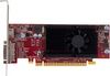
NVIDIA GeForce GT 625 vs NVIDIA GeForce GTX 645 Full Specs
48 Shaders 810MHz | 576 Shaders 889MHz |
524MB DDR314.4GB/s | 1GB GDDR564GB/s |
·· 155.5 GFLOPS | ·· 1.02 TFLOPS |
Form Factor PCIe Card | Form Factor PCIe Card |
TDP 30W | TDP 64W |
 GeForce GT 625155.5 GFLOPSFP32
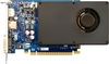 GeForce GTX 6451.02 TFLOPSFP32
Clock Speed ·· | Clock Speed ··· |
Peak OPS 155.5 GFLOPSFP32 | Peak OPS 1.02 TFLOPSFP32 |
FP32 155.5 GFLOPS | FP32 1.02 TFLOPS |
FP64 12.96 GFLOPS | FP64 42.67 GFLOPS |
Pixel Rate 6.5 GPixel/s | Pixel Rate 14.2 GPixel/s |
Texture Rate 13 GTexel/s | Texture Rate 42.7 GTexel/s |
Shaders 48 Shaders | Shaders 576 Shaders |
TMUs 8 TMUs | TMUs 48 TMUs |
ROPs 4 ROPs | ROPs 16 ROPs |
SM 1 SM | SMs 3 SMs |
Base Clock - | Base Clock 824MHz |
Boost Clock 810MHz | Boost Clock 889MHz |
Shader Clock 1.62GHz | Shader Clock - |
L2 Cache 128KB shared | L2 Cache 512KB shared |
524MB DDR3 | 1GB GDDR5 |
Memory Bus 64-bit | Memory Bus 128-bit |
Memory Speed 1.8GT/s | Memory Speed 4GT/s |
Memory Bandwidth 14.4GB/s | Memory Bandwidth 64GB/s |
TDP 30W | TDP 64W |
Multi-Monitor 2 | Multi-Monitor 2 |
- | 1x DisplayPort 1.2 |
- | 1x HDMI 1.4 |
1x HDMI 1.3 | - |
1x DVI-I Dual-Link | 1x DVI-I Dual-Link |
- | Encoder Model NVENC 1 |
Decoder Model VP5 | Decoder Model NVDEC 1 |
Form Factor PCIe Card | Form Factor PCIe Card |
PCIe 1-Slots | PCIe 1-Slots |
Height 69 mm (2.72")Width 155 mm (6.1")Depth 20 mm (0.79") | Height 111 mm (4.37")Width 168 mm (6.61")Depth 20 mm (0.79") |
Cooling Open-Air 1x Fan | Cooling Blower 1x Fan |
Manufacturer | Manufacturer |
Chip Designer | Chip Designer |
Architecture | Architecture |
Family | Family |
Branding  | Branding |
Codename NVD9 | Codename NVE6 |
Market Segment Desktop | Market Segment Desktop |
Release Date Feb 19, 2013 | Release Date Apr 22, 2013 |
Foundry TSMC | Foundry TSMC |
Fabrication Node 40nm | Fabrication Node 28nm |
Die Size 79mm² | Die Size 221mm² |
Transistor Count 292 Million | Transistor Count 2.5 Billion |
Transistor Density 3.7 MTr/mm² | Transistor Density 11.49 MTr/mm² |
No images available
No images available