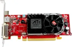
Radeon HD 3450
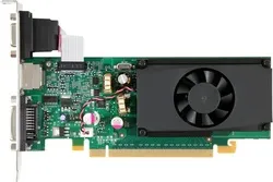
GeForce 210
ATI Radeon HD 3450 vs NVIDIA GeForce 210 Full Specs
40 Shaders 600MHz | 16 Shaders 520MHz |
256MB DDR28GB/s | 512MB DDR24GB/s |
·· 48 GFLOPS | ·· 44.86 GFLOPS |
Form Factor PCIe Card | Form Factor PCIe Card |
TDP 25W | TDP 31W |
 Radeon HD 345048 GFLOPSFP32
 GeForce 21044.86 GFLOPSFP32
Clock Speed ·· | Clock Speed ·· |
Peak OPS 48 GFLOPSFP32 | Peak OPS 44.86 GFLOPSFP32 |
FP32 48 GFLOPS | FP32 44.86 GFLOPS |
Pixel Rate 2.4 GPixel/s | Pixel Rate 5.6 GPixel/s |
Texture Rate 2.4 GTexel/s | Texture Rate 11.2 GTexel/s |
Shaders 40 Shaders | Shaders 16 Shaders |
TMUs 4 TMUs | TMUs 8 TMUs |
ROPs 4 ROPs | ROPs 4 ROPs |
CUs 2 CUs | SMs 2 SMs |
Boost Clock 600MHz | Boost Clock 520MHz |
Shader Clock - | Shader Clock 1.4GHz |
L1 32KB/4SPs | L1 16KB/SM Tex |
L2 Cache 64KB shared | L2 Cache 32KB shared |
256MB DDR2 | 512MB DDR2 |
Memory Bus 64-bit | Memory Bus 32-bit |
Memory Speed 1GT/s | Memory Speed 1GT/s |
Memory Bandwidth 8GB/s | Memory Bandwidth 4GB/s |
ECC No | ECC No |
TDP 25W | TDP 31W |
Max Resolution 2560x1600 | Max Resolution 2560x1600 |
Refresh Rate Calculator 2560x1440 Resolution1440p QHD Refresh Rate 66Hz | Refresh Rate Calculator 2560x1440 Resolution1440p QHD Refresh Rate 66Hz |
Multi-Monitor 2 | Multi-Monitor 2 |
DSC Not Supported | DSC Not Supported |
- 1x DVI-I Dual-Link 1x S-Video | 1x DisplayPort 1.0 1x DVI-I Dual-Link 1x VGA |
Shader Model 4.1 | Shader Model 4 |
DirectX DirectX 10Direct3D 10_1 | DirectX DirectX 11Direct3D 10_0 |
OpenGL 3.3OpenCL 1.1 | OpenGL 3.3OpenCL 1.1 |
CUDA -GFX 3PureVideo HD -VDPAU - | CUDA 1.2GFX -PureVideo HD VP4VDPAU Feature Set C |
Decoder UVD 1.0 | Decoder VP4 |
Codec VC-1 AVC (H.264) | Codec - |
Form Factor PCIe Card | Form Factor PCIe Card |
PCIe PCIe 2.0 x16 1-Slots | PCIe PCIe 2.0 x16 1-Slots |
- | Height 69mm (2.72")Width 168mm (6.61")Depth 20mm (0.79") |
Cooling Open-Air 1x Fan | Cooling Open-Air 1x Fan |
Multi-GPU - | Multi-GPU Multi-GPU Support SupportedMulti-GPU Type 2-way SLI |
Manufacturer | Manufacturer |
Chip Designer | Chip Designer |
Architecture | Architecture |
Family | Family |
Branding  | Branding  |
Codename Koopa | Codename NVA8 |
Chip Variant RV620 LE | Chip Variant 8400GS-225-B1 |
Market Segment Desktop | Market Segment Desktop |
Release Date Jan 23, 2008 | Release Date Oct 12, 2009 |
Foundry TSMC | Foundry TSMC |
Fabrication Node 55nm | Fabrication Node 40nm |
Die Size 67mm² | Die Size 57mm² |
Transistor Count 181M | Transistor Count 260M |
Transistor Density 2.7 MTr/mm² | Transistor Density 4.56 MTr/mm² |