AMD Radeon E9175 vs AMD Radeon E9260 Full Specs
512 Shaders 1.22GHz | 896 Shaders 1.22GHz |
4GB GDDR596GB/s | 4GB GDDR5112GB/s |
·· 1.25 TFLOPS | ·· 2.18 TFLOPS |
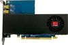
Form Factor PCIe Card | Form Factor MXM-A |
TDP 50W | TDP 80W |
 Radeon E91751.25 TFLOPSFP16
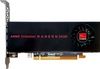 Radeon E92602.18 TFLOPSFP16
Clock Speed ··· | Clock Speed ··· |
Peak OPS 1.25 TFLOPSFP16 | Peak OPS 2.18 TFLOPSFP16 |
FP32 1.25 TFLOPS | FP32 2.18 TFLOPS |
FP64 78.02 GFLOPS | FP64 136.5 GFLOPS |
Pixel Rate 19.5 GPixel/s | Pixel Rate 19.5 GPixel/s |
Texture Rate 39 GTexel/s | Texture Rate 58.5 GTexel/s |
Shaders 512 Shaders | Shaders 896 Shaders |
TMUs 32 TMUs | TMUs 48 TMUs |
ROPs 16 ROPs | ROPs 16 ROPs |
CUs 8 CUs | CUs 14 CUs |
Base Clock 1.12GHz | Base Clock 1.12GHz |
Boost Clock 1.22GHz | Boost Clock 1.22GHz |
L2 Cache 512KB shared | L2 Cache 1MB shared |
4GB GDDR5 | 4GB GDDR5 |
Memory Bus 128-bit | Memory Bus 128-bit |
Memory Speed 6GT/s | Memory Speed 7GT/s |
Memory Bandwidth 96GB/s | Memory Bandwidth 112GB/s |
TDP 50W | TDP 80W |
Multi-Monitor 3 | Multi-Monitor 3 |
HDCP HDCP 2.2 | HDCP HDCP 2.2 |
Encoder Model VCE 3.4 | Encoder Model VCE 3.4 |
Decoder Model UVD 6.3 | Decoder Model UVD 6.3 |
Form Factor PCIe Card | Form Factor MXM-A |
Cooling Passive | Cooling Passive |
Manufacturer | Manufacturer |
Chip Designer | Chip Designer |
Architecture | Architecture |
Family | Family |
Branding  | Branding |
Codename Lexa | Codename Baffin |
Chip Variant Polaris 12 XL | Chip Variant Polaris 11 XL |
Market Segment Server | Market Segment Server |
Release Date Oct 1, 2017 | Release Date Sep 1, 2016 |
Foundry GlobalFoundries | Foundry GlobalFoundries |
Fabrication Node 14LPP | Fabrication Node 14LPP |
Die Size 103mm² | Die Size 123mm² |
Transistor Count 2.2 Billion | Transistor Count 3 Billion |
Transistor Density 21.36 MTr/mm² | Transistor Density 24.39 MTr/mm² |
No images available
No images available