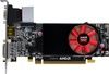
AMD Radeon R5 230 vs AMD Radeon R9 295X2 Full Specs
160 Shaders 625MHz | 5,632 Shaders 1.02GHz |
1GB DDR38.5GB/s | 8GB GDDR5640GB/s |
·· 200 GFLOPS | ·· 11.47 TFLOPS |
Form Factor PCIe Card | Form Factor PCIe Card |
TDP 19W | TDP 500W |
Power Connectors - | Power Connectors 2x 8-Pin |
 Radeon R5 230200 GFLOPSFP32
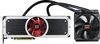 Radeon R9 295X211.47 TFLOPSFP32 (2x 5.73 TFLOPS)
Clock Speed ·· | Clock Speed ·· |
Peak OPS 200 GFLOPSFP32 | Peak OPS 11.47 TFLOPSFP32 |
FP32 200 GFLOPS | FP32 11.47 TFLOPS |
- | FP64 1.43 TFLOPS |
Pixel Rate 2.5 GPixel/s | Pixel Rate 65.2 GPixel/s |
Texture Rate 5 GTexel/s | Texture Rate 179.2 GTexel/s |
Shaders 160 Shaders | Shaders 5,632 Shaders |
TMUs 8 TMUs | TMUs 352 TMUs |
ROPs 4 ROPs | ROPs 128 ROPs |
CUs 2 CUs | CUs 88 CUs |
Boost Clock 625MHz | Boost Clock 1.02GHz |
L2 Cache 128KB shared | L2 Cache 1MB shared |
1GB DDR3 | 8GB GDDR5 |
Memory Bus 64-bit | Memory Bus 512-bit |
Memory Speed 1.1GT/s | Memory Speed 5GT/s |
Memory Bandwidth 8.5GB/s | Memory Bandwidth 640GB/s |
TDP 19W | TDP 500W |
Multi-Monitor 2 | Multi-Monitor 4 |
HDCP - | HDCP HDCP 1.4 |
- | 4x Mini DisplayPort 1.2 |
1x HDMI 1.3 | - |
- | 1x DVI-D Dual-Link |
1x DVI-I Dual-Link | - |
- | Encoder Model VCE 2.0 |
Decoder Model UVD 3.0 | Decoder Model UVD 4.2 |
Form Factor PCIe Card | Form Factor PCIe Card |
PCIe 1-Slots | PCIe 2.1-Slots |
- | Height 115 mm (4.53")Width 307 mm (12.09")Depth 42 mm (1.65") |
Cooling Open-Air 1x Fan | Cooling Liquid 120mm Radiator 1x Fan |
Power Connectors - | Power Connectors 2x 8-Pin |
Manufacturer | Manufacturer |
Chip Designer | Chip Designer |
Architecture | Architecture |
Family | Family |
Branding  | Branding |
Codename Caicos | Codename Hawaii |
Chip Variant Caicos | Chip Variant Hawaii Pro |
Market Segment Desktop | Market Segment Desktop |
Release Date Apr 3, 2014 | Release Date Apr 8, 2014 |
Foundry TSMC | Foundry TSMC |
Fabrication Node 40nm | Fabrication Node 28nm |
Die Size 67mm² | Die Size 438mm² |
Transistor Count 370 Million | Transistor Count 6.2 Billion |
Transistor Density 5.52 MTr/mm² | Transistor Density 14.16 MTr/mm² |
No images available
No images available