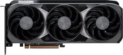
Radeon RX 9070 XT
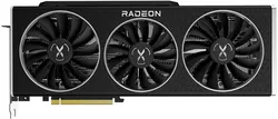
Radeon RX 6800 XT Speedster MERC 319
AMD Radeon RX 9070 XT vs XFX Radeon RX 6800 XT Speedster MERC 319 Full Specs
4,096 Shaders 2.97GHz | 4,608 Shaders 2.25GHz |
16GB GDDR6640GB/s | 16GB GDDR6512GB/s |
·· 48.66 TFLOPS | ·· 20.74 TFLOPS |
Form Factor PCIe Card | Form Factor PCIe Card |
TDP 304W | TDP 300W |
Power Connectors 2x 8-Pin | Power Connectors 2x 8-Pin |
 Radeon RX 9070 XT1.56 POPSINT4 Tensor Sparse
 Radeon RX 6800 XT Speedster MERC 31941.47 TFLOPSFP16
Clock Speed ··· | Clock Speed ··· |
Peak OPS 1.56 POPSINT4 Tensor Sparse | Peak OPS 41.47 TFLOPSFP16 |
Tensor FP8-16 194.6 TFLOPSFP8-16 Tensor Sparse 389.3 TFLOPSTensor FP8-32 194.6 TFLOPSFP8-32 Tensor Sparse 389.3 TFLOPS | - |
Tensor FP16-16 97.32 TFLOPSFP16-16 Tensor Sparse 194.6 TFLOPSTensor FP16-32 97.32 TFLOPSFP16-32 Tensor Sparse 194.6 TFLOPS | - |
BF16 97.32 TFLOPSTensor BF16 97.32 TFLOPSBF16 Tensor Sparse 194.6 TFLOPS | - |
FP32 48.66 TFLOPS | FP32 20.74 TFLOPS |
FP64 1.52 TFLOPS | FP64 1.3 TFLOPS |
Tensor INT4 778.6 TOPS | Tensor INT4 - |
Tensor INT8 389.3 TOPS | - |
Pixel Rate 380.2 GPixel/s | Pixel Rate 288 GPixel/s |
Texture Rate 760.3 GTexel/s | Texture Rate 648 GTexel/s |
Shaders 4,096 Shaders | Shaders 4,608 Shaders |
TMUs 256 TMUs | TMUs 288 TMUs |
ROPs 128 ROPs | ROPs 128 ROPs |
Tensor Cores 128 T-Cores | Tensor Cores - |
RT Cores 64 RT-Cores | RT Cores 72 RT-Cores |
CUs 64 CUs | CUs 72 CUs |
Base Clock 2.4GHz | Base Clock 1.82GHz |
Boost Clock 2.97GHz | Boost Clock 2.25GHz |
L0 Cache 64KB/WGP | L0 Cache 32KB/WGP |
L1 256KB/Array | L1 128KB/Array |
L2 Cache 8MB shared | L2 Cache 4MB shared |
L3 Cache 64MB shared | L3 Cache 128MB shared |
L3 Bandwidth 2.25TB/s | L3 Bandwidth 1.66TB/s |
16GB GDDR6 | 16GB GDDR6 |
Memory Bus 256-bit | Memory Bus 256-bit |
Memory Speed 20GT/s | Memory Speed 16GT/s |
Memory Bandwidth 640GB/s | Memory Bandwidth 512GB/s |
ECC No | ECC No |
TDP 304W | TDP 300W |
Max Temp - | Max Temp 110°C Max |
Max Resolution 7680x4320 | Max Resolution 7680x4320 |
Refresh Rate Calculator 7680x4320 Resolution8K UHD Refresh Rate 165Hz | Refresh Rate Calculator 7680x4320 Resolution8K UHD Refresh Rate 120Hz |
Multi-Monitor 3 | Multi-Monitor 4 |
Adaptive Sync FreeSync | Adaptive Sync FreeSync |
DSC Supported | DSC Supported |
HDCP HDCP 2.3 | HDCP HDCP 2.3 |
3x DisplayPort 2.1 1x HDMI 2.1 | 3x DisplayPort 1.4 1x HDMI 2.1 |
Shader Model 6.8 | Shader Model 6.5 |
DirectX DirectX 12Direct3D 12_2 | DirectX DirectX 12Direct3D 12_2 |
OpenGL 4.6OpenCL 2.2Vulkan 1.3 | OpenGL 4.6OpenCL 2.1Vulkan 1.2 |
GFX 12 | GFX 10.3 |
Encoder VCN 4.0 | Encoder VCN 3.0 |
Codec VP9 AVC (H.264) HEVC (H.265) AV1 | Codec - AVC (H.264) HEVC (H.265) - |
Decoder VCN 4.0 | Decoder VCN 3.0 |
Codec MPEG-1 MPEG-2 MPEG-4 JPEG VC-1 VP9 AVC (H.264) HEVC (H.265) AV1 | Codec MPEG-1 MPEG-2 MPEG-4 JPEG VC-1 VP9 AVC (H.264) HEVC (H.265) AV1 |
Form Factor PCIe Card | Form Factor PCIe Card |
PCIe PCIe 5.0 x16 2.5-Slots | PCIe PCIe 4.0 x16 2.7-Slots |
Height 111mm (4.37")Width 267mm (10.51")Depth 50mm (1.97") | Height 138mm (5.43")Width 340mm (13.39")Depth 54mm (2.13") |
Cooling Open-Air 3x Fans | Cooling Open-Air 3x Fans |
Power Connectors 2x 8-Pin | Power Connectors 2x 8-Pin |
Multi-GPU Multi-GPU Support SupportedMulti-GPU Type CrossFire XDMA | Multi-GPU Multi-GPU Support SupportedMulti-GPU Type Bridgeless |
Manufacturer | Manufacturer |
Chip Designer | Chip Designer |
Architecture | Architecture |
Family | Family |
Branding  | Branding  |
Codename - | Codename Sienna Cichlid |
Chip Variant Navi 48 XL | Chip Variant Navi 21 XL |
Market Segment Desktop | Market Segment Desktop |
Release Date Jan 6, 2025 | Release Date Nov 18, 2020 |
Foundry TSMC | Foundry TSMC |
Fabrication Node N4P | Fabrication Node N7 |
Die Size 357mm² | Die Size 520mm² |
Transistor Count 53.9B | Transistor Count 26.8B |
Transistor Density 151.2 MTr/mm² | Transistor Density 51.56 MTr/mm² |