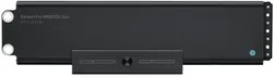
Radeon Pro W6800X Duo
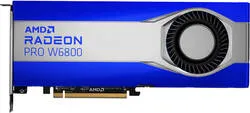
Radeon PRO W6800
Apple Radeon Pro W6800X Duo vs AMD Radeon PRO W6800 Full Specs
7,680 Shaders 1.97GHz | 3,840 Shaders 2.32GHz |
64GB GDDR61.02TB/s | 32GB GDDR6512GB/s |
·· 30.26 TFLOPS | ·· 17.82 TFLOPS |
Form Factor MPX | Form Factor PCIe Card |
TDP 400W | TDP 250W |
Power Connectors - | Power Connectors 1x 8-Pin 1x 6-Pin |
 Radeon Pro W6800X Duo60.52 TFLOPSFP16 (2x 30.26 TFLOPS)
 Radeon PRO W680035.64 TFLOPSFP16
Clock Speed ··· | Clock Speed ··· |
Peak OPS 60.52 TFLOPSFP16 | Peak OPS 35.64 TFLOPSFP16 |
FP32 30.26 TFLOPS | FP32 17.82 TFLOPS |
FP64 1.89 TFLOPS | FP64 1.11 TFLOPS |
Pixel Rate 189.1 GPixel/s | Pixel Rate 222.7 GPixel/s |
Texture Rate 472.8 GTexel/s | Texture Rate 556.8 GTexel/s |
Shaders 7,680 Shaders | Shaders 3,840 Shaders |
TMUs 480 TMUs | TMUs 240 TMUs |
ROPs 192 ROPs | ROPs 96 ROPs |
RT Cores 120 RT-Cores | RT Cores 60 RT-Cores |
CUs 120 CUs | CUs 60 CUs |
Base Clock 1.8GHz | Base Clock 2.08GHz |
Boost Clock 1.97GHz | Boost Clock 2.32GHz |
L0 Cache 32KB/WGP | L0 Cache 32KB/WGP |
L1 128KB/Array | L1 128KB/Array |
L2 Cache 4MB shared | L2 Cache 4MB shared |
L3 Cache 128MB shared | L3 Cache 128MB shared |
L3 Bandwidth 1.66TB/s | L3 Bandwidth 1.66TB/s |
64GB GDDR6 | 32GB GDDR6 |
Memory Bus 256-bit | Memory Bus 256-bit |
Memory Speed 16GT/s | Memory Speed 16GT/s |
Memory Bandwidth 1.02TB/s | Memory Bandwidth 512GB/s |
ECC No | ECC No |
TDP 400W | TDP 250W |
Max Temp 100°C Max | Max Temp - |
Max Resolution 7680x4320 | Max Resolution 7680x4320 |
Refresh Rate Calculator 7680x4320 Resolution8K UHD Refresh Rate 120Hz | Refresh Rate Calculator 7680x4320 Resolution8K UHD Refresh Rate 120Hz |
Multi-Monitor 8 | Multi-Monitor 4 |
Adaptive Sync FreeSync | Adaptive Sync FreeSync |
DSC Supported | DSC Supported |
HDCP HDCP 2.3 | HDCP HDCP 2.3 |
- 1x HDMI 2.0 4x Thunderbolt 3 | 6x Mini DisplayPort 1.4 - - |
Shader Model 6.5 | Shader Model 6.5 |
DirectX DirectX 12Direct3D 12_2 | DirectX DirectX 12Direct3D 12_2 |
OpenGL 4.6OpenCL 2.1Vulkan 1.2 | OpenGL 4.6OpenCL 2.1Vulkan 1.2 |
GFX 10.3 | GFX 10.3 |
Encoder VCN 3.0 | Encoder VCN 3.0 |
Codec AVC (H.264) HEVC (H.265) | Codec AVC (H.264) HEVC (H.265) |
Decoder VCN 3.0 | Decoder VCN 3.0 |
Codec MPEG-1 MPEG-2 MPEG-4 JPEG VC-1 VP9 AVC (H.264) HEVC (H.265) AV1 | Codec MPEG-1 MPEG-2 MPEG-4 JPEG VC-1 VP9 AVC (H.264) HEVC (H.265) AV1 |
Form Factor MPX | Form Factor PCIe Card |
PCIe PCIe 4.0 x16 4-Slots | PCIe PCIe 4.0 x16 2-Slots |
- | Height 111mm (4.37")Width 267mm (10.51")Depth 40mm (1.57") |
Cooling Passive - | Cooling Blower 1x Fan |
Power Connectors - | Power Connectors 1x 8-Pin, 1x 6-Pin |
Multi-GPU Multi-GPU Support SupportedMulti-GPU Type Bridgeless | Multi-GPU Multi-GPU Support SupportedMulti-GPU Type Bridgeless |
Manufacturer | Manufacturer |
Chip Designer | Chip Designer |
Architecture | Architecture |
Family | Family |
Branding  | Branding |
Codename Sienna Cichlid | Codename Sienna Cichlid |
Chip Variant Navi 21 XL | Chip Variant Navi 21 XL |
Market Segment Workstation | Market Segment Workstation |
Release Date Aug 3, 2021 | Release Date Jun 8, 2021 |
Foundry TSMC | Foundry TSMC |
Fabrication Node N7 | Fabrication Node N7 |
Die Size 520mm² | Die Size 520mm² |
Transistor Count 26.8B | Transistor Count 26.8B |
Transistor Density 51.56 MTr/mm² | Transistor Density 51.56 MTr/mm² |
Desktops | Desktops - |